Search
Star
Feedback
Setup for Free
© 2026 Hedgehog Software, LLC
Twitter
GitHub
Discord
System
Light
Dark
More
Communities
Docs
About
Terms
Privacy
@Seve seve is this good onyl width - tscircuit
t
tscircuit
•
8mo ago
•
144 replies
ansh.grover
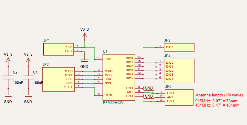
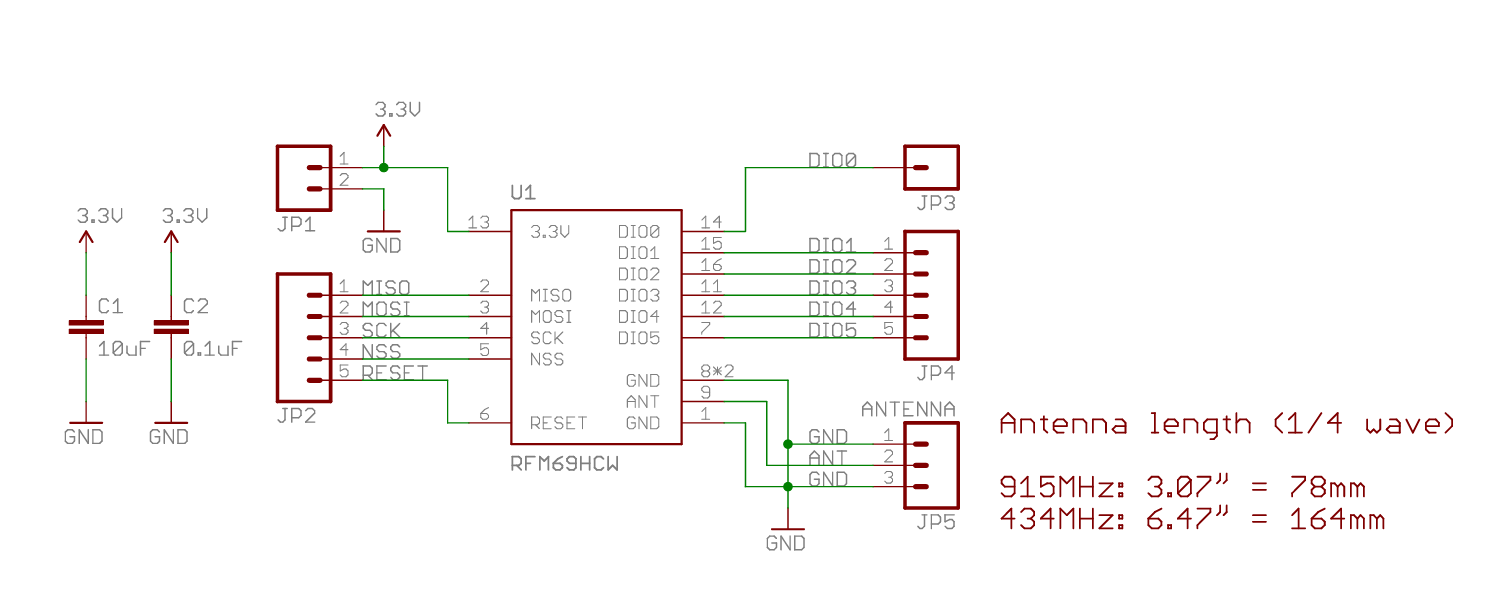
@Seve seve is this good onyl width
@Seve seve is this good onyl width issue
, done added the netlabels instead of that netalias in JP1 as said by you
.
tscircuit
Join
The community & user server for tscircuit. Build electronics with React & AI. Render code into schematics, PCBs, 3D, fabrication files, and more.
487
Members
View on Discord
Resources
ModelContextProtocol
ModelContextProtocol
MCP Server
Recent Announcements
Similar Threads
Was this page helpful?
Yes
No
Next page
Similar Threads
Seve - this is a good pretty hard one: https://...
t
tscircuit / contributor
4mo ago
Seve - this is a good feature for ground pours ...
t
tscircuit / contributor
4mo ago
DOPΣ - @Seve is this alr?
t
tscircuit / contributor
2mo ago
Anas - @Seve Panelization width and hight
t
tscircuit / contributor
3mo ago