3-lead chip antenna identification (continued from hardware-help)
Ok, let's move the discussion here so it's easier to track....
15 Replies
https://pcbartists.com/design/rf/chip-antenna-pcb-layout-bluetooth-wifi/amp/
Here's an article that may prove helpful during your (re)design process...
PCB Artists
Chip Antenna PCB Layout (Bluetooth and Wi-Fi) - PCB Artists
An illustrated article on chip antenna PCB layout with focus on 2.4 GHz WiFi and Bluetooth antennas. Applicable to ESP32, ESP8266, nRF52, etc.
@Pykess
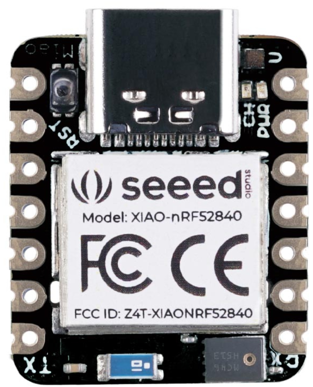
looking at this photo....the antenna chip in question MAY WELL BE a 4-lead model, just like the one in the article:
Unknown User•3y ago
Message Not Public
Sign In & Join Server To View
looks kinda like a solder-blob fusing 2 pins together, to my eye
...which would make those 2 pins GND
Unknown User•3y ago
Message Not Public
Sign In & Join Server To View
...leaving only 2-pins to figure out...SIG & CAP 😉
if this antenna matches the one in the PCB Artists article, the upper-right pin/pad would be SIG, but I'm still trying to find more data to confirm that with.
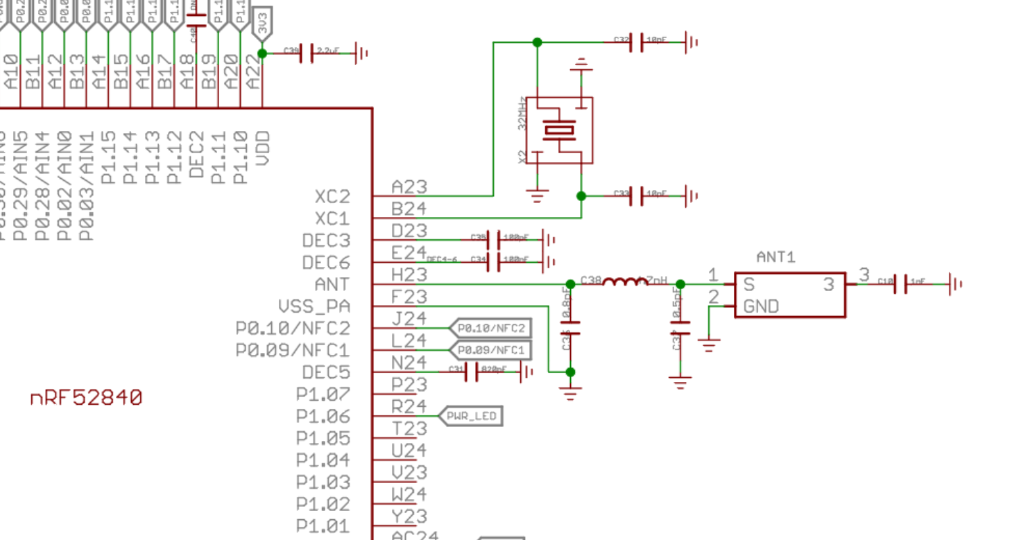
https://files.seeedstudio.com/wiki/XIAO-BLE/Seeed-Studio-XIAO-nRF52840-Sense-v1.1.pdf
why is noone looking into the schematics for this
I hadn't gotten to there yet, but pykess was trying to figure out which pin is which, in order to desolder the chip antenna & attach an adapter for an aerial antenna in its place
but from that schematic, it almost looks like the 2 shorted leads are going to the capacitor?
Unknown User•3y ago
Message Not Public
Sign In & Join Server To View
what are the resistances?
Unknown User•3y ago
Message Not Public
Sign In & Join Server To View
sounds about right