Custom motor driver module
I am planning to make a high current motor driver module with IRLZ34NPBF mosfets. But I am wondering what components to add to make a nicely working system, like resistors, capacitors, and diodes. I know I need a 10k resistor for the gate to ground, and I know I need diodes from the drain to the vcc. But is there anything else I should have other than those?
611 Replies
Capacitors....both poly-caps for storage & ceramics for suppressing transients & decoupling.
thank you. would the ceramic capacitors go across the would-be leads of the motors? and the electrolytic capacitors go from vcc to ground?
well, for starters you'll want at least one polymer and 2 ceramics from Vcc to GND, with minimum ESR on the ceramics, and both different sizes that are NOT multiples of each other.
after that, things depend a lot more on the specifics of your design.
okay thank you very much, I will come back with a schematic/pcb design sometime
I have seen some boards with 4.7uf and 0.1uf capacitors for decoupling, but wouldn't those be multiples of each other
well, 47:1 is enough of a whacko multiple that those should be fine.
meanwhile, 2:1, 3:1, 5:1, and pretty much anything below 16:1 would be likely to cause potential resonance issues.
Here is my schematic so far:

I have 2 ceramics and a polarized capacitor at the bottom, a 10k pull-down resistor on the gate, and a flyback diode on the drain
I am also not sure what values I should be using for the poly cap
GND connections should always, ALWAYS point down ... otherwise they become ANTenna emblems on the schematic.
idk, if you have a 10uF ceramic already, maybe use a 470nF and a 22nF cap to go with it.
Okay thank you very much, I did not know this 😅
...if you still just wanted to "go for it" with a poly storage cap "to top it all off", maybe drop a 390uF poly on there just for good measure
do you mean, a 10uf ceramic, a 22nf ceramic, and a 470nf polymer?
and no others?
470nF is far too small for poly-cap. that one will be ceramic too
I think I will do this too haha
Could I just use 2 of those ceramic caps and the poly cap, instead of 3 of the ceramic caps and a poly?
it's up to you. I use 0603-format ceramic chip-capacitors. They're small enough to fit 50 on a US quarter, and cheap as everything too, so no real reason to "be stingy with them"
Okay thank you. I'll think about it
though if I do decide to use 2 instead of 3 ceramics, should I pick the 10uf and 22nf?
one very small and one a good bit larger?
I'd prob. do the 10uF & the 470nF, unless you're expecting some rlly high-frequency noise in the system.
Alright thanks! I am planning to use the QWIIC system on the board too, that wouldn't make any unwanted noise right?
shared GND but not VCC
if that matters
well, the decoupling caps are usually more for "local VCC noise", like for rlly high-speed digital chips & what-not
...still need decouplers for basically anything you want a square-wave output from, just not the really, REALLY low value ones.
Alright sounds good
and how about the voltage for the polymer capacitor
the max voltage on the mosfet is 30v, so should the poly cap be rated for at least that?
incase I want to use 30 volts for the motor
Yes, the LAST THING you want to do is charge that poly up past its rated max voltage .... so until raising the voltage makes the cap "too expensive" or "too big for the board", higher is better.
okay, I went with 40v instead of 35v haha
now for the temperature
I am hoping to maybe get a max current of 40 amps, and at a max copper trace temperature of 40C I would need 20mm wide traces
But I want to add a heat sink, im just not sure how I should implement it. Could I lay the mosfet down flat on the pcb (and solder the top tab to the board) then have a heat sink on the other side of the pcb?
maybe use 2oz copper, or forced convection cooling
2oz of copper will cost way too much for me
I would like to just use a heatsink or two
ok
Would I be able to lay the mosfet down on the pcb with vias and have the heatsink on the other side?
with enough thermal vias, yes... that's what they do with all the TMC-based stepperstick boards
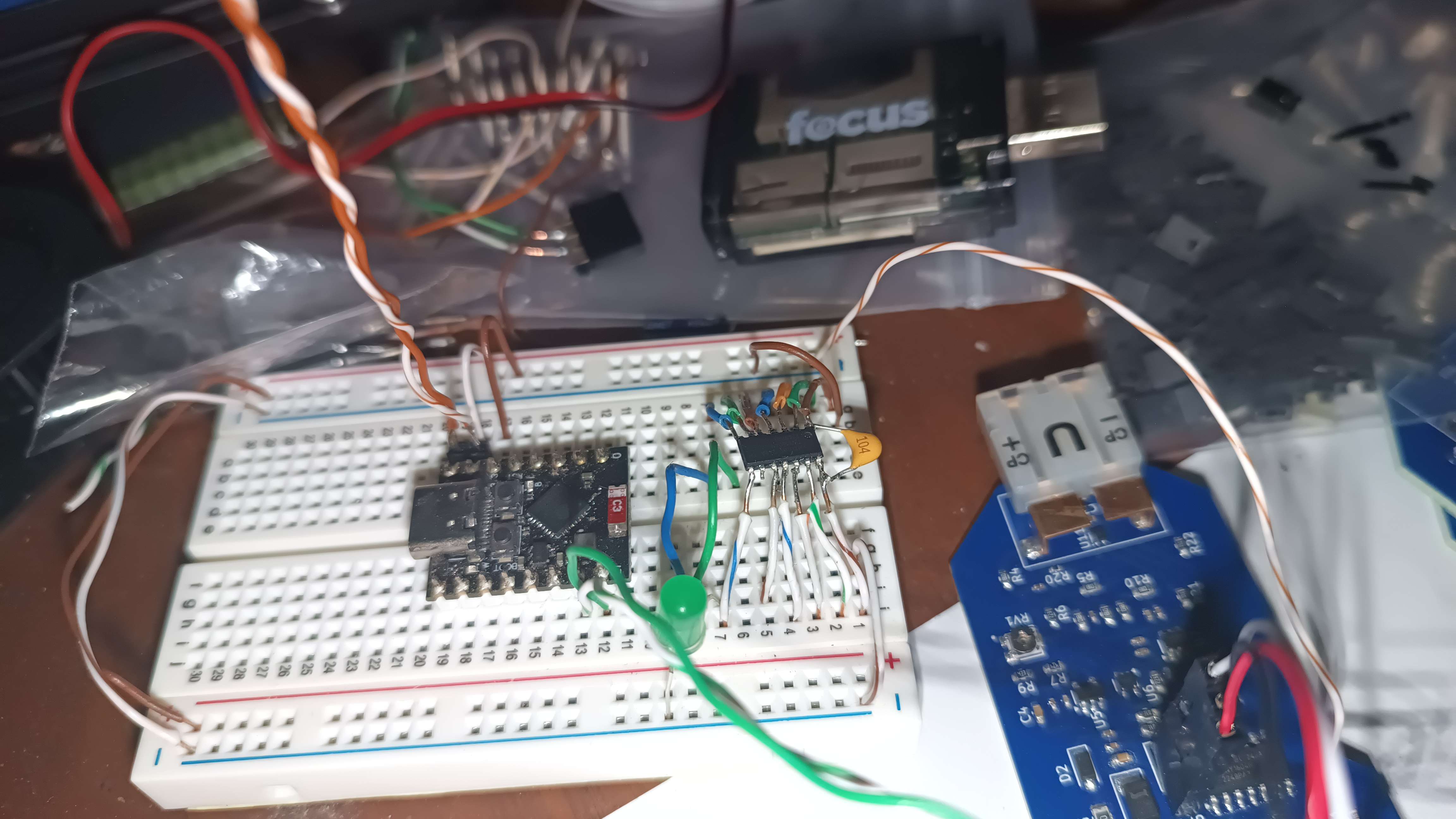
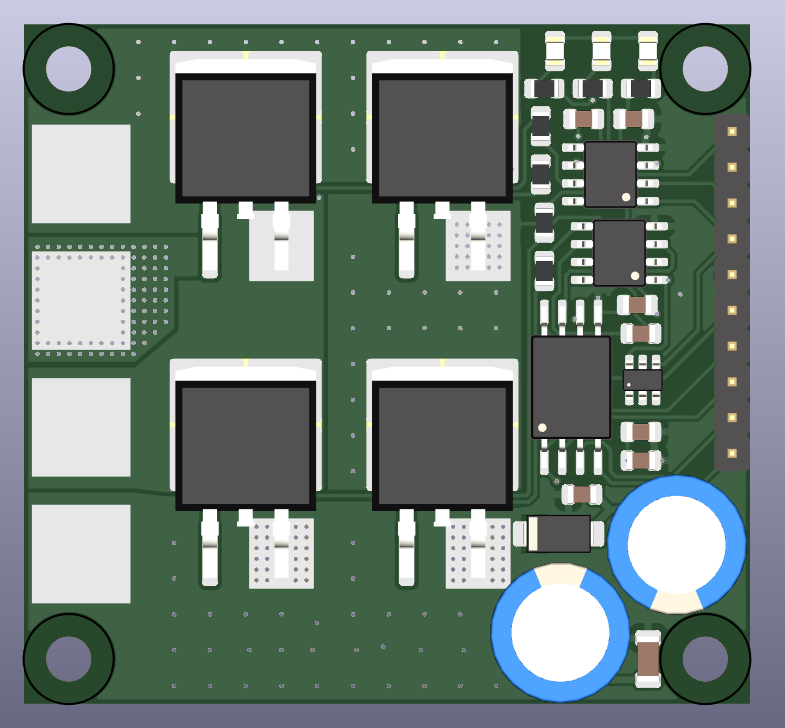
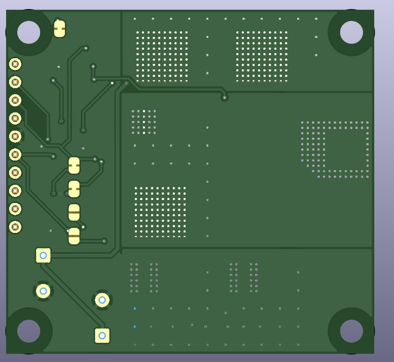
here is my current pcb layout:


I have that big grid of vias under the mosfet to the other side of the board
I also just realized, when I put the heatsink on the back of the board It is going to short circuit all of those bare power pads, is there anything I can do to stop that from happening
you can use a smaller-footprint heatsink, or put something electrically insulative (like a glass/ceramic wafer) and thermally conductive over them before installing a larger heatsink (assuming there won't be any tht leads protruding through those holes)
hmm, I might just cut out the pairs of screw terminals I have and just leave the THT pads for wire too be soldered to, that way I can put the heatsink over more area, and hopefully not need to insulate it anymore
could use one of the little vertical-heatsinks for stepper drivers
like these: https://a.aliexpress.com/_mqzqPEb
I would do this, but the copper traces should be getting pretty hot too, so I think having a heatsink over those will help
I ended up just taking the THT pads out and adding large SMD pads


and if I cut the leads on the mosfet short, I should be able to stick a heatsink back there nicely
here is my final design:

If you have anymore suggestions I would be happy to hear them
any way you could switch places between these 2 components? (or at least rotate the white connector 90° clockwise, to allow moving the THT ISP pins further away from the FET backside where the heatsink goes).
would I just do this so I could fit the heatsink in without trimming the pins?
you wanted max-coverage from the heatsink, so I mentioned something I saw that could allow you to more easily mount a bigger heatsink 😁
okay so you are talking about that
originally I was planning on maybe soldering header pins in there, but I decided that I could just temporarily stick pins into those pads to program the microchip, instead of soldering them in permanently. so really in the end those pads wont really "be there"
and they aren't exposed at the back either so I shouldn't have any short circuit problems
??? sooo, you're taking the THT pins out of the design & replacing them with surface-pads on the front, to use with a pogo-pin adaptor?
no sorry, i am leaving the THT pads as-is, just not having any solder mask on the back and not soldering anything to them
if that makes sense
you'll hate yourself for that decision, I predict
(unsoldered header pins are a big no-no)
yeah, I just figured since I would only need to program with them once or twice, I don't need to permanently solder pins in
I also have an soic-8 clip I can use to program the attiny85 if I do really hate the alternate way
but that's why I gave you "a better option"
well I haven't really messed around with them before
maybe this can be a project to try them out on
on your pcb, you just have to put 6 bare pads (like test-point pads)
...then you just order another tiny PCB with 6 pogo-pins & a regular ICSP 6-pin header & maybe 3d print a holder to clip your board onto it while programming.
alright thanks, i can make the pogo pin board tomorrow haha
I noticed sparkfun uses small THT pads for the pogo pins to sit, I guess that helps with keeping them aligned
THT pads would have no solder-mask on the back side, so could short to the heatsink
Well I could have the pads covered up on that side and leave the other side bare
who is making the PCBs?
Jlcpcb
and they've agreed to these requirements???
I mean that's how I've designed it
they just don't put any solder mask there like any other part of the board
well, if the solder-mask covers the bottoms, great...I'll wait to see the pictures when you receive the boards 😂
well im sure I can find a way to cover them if they don't put solder mask there
here is the now final design:


I am planning to solder on these to connect wires easier

Might need a welder for that 😂
why not use screw terminals with PCB mounting pins?
(to make them far easier to solder on)
The ones for 8 gauge or smaller are really really big seems
I may not be looking for the right thing though
I don't see any traces on your PCB that can handle enough current to warrant 8ga wires tho
tbf, it looks like the middle-leg on your transistor is left floating.
well, the board should get pretty hot with the even with the heatsink of course, but might as well keep the wires from getting that hot if possible
I might be looking at something wrong, but it looks to me like the 2 middle pads (+ & VCC) are connected to 1 diode & 3 capacitors....and nothing else.
that's correct, I could figure out a way to connect it, but I though the tab would be enough, do you think I should connect it too?
that's right
ahh, if the tab is internally connected to pin2, that should be fine.
how does that work, then?
nothing needs referred to motor VCC, so you're doing everything based on GND and data VCC?
I will double check
one lead of the motor is directly connected to VCC, and the other lead is connected to the mosfet's drain
and everything as a common GND
ok, so "-" is the switched line to the motor (MOSFET Drain)?
That's right
ok, then now that my brain's no longer screaming "this does not compute", I think as long as those lugs are mickel or tin coated, you should probably be able to solder them on a hotplate, with maybe an iron on top of the lug too (solder the lugs BEFORE any of the temperature-sensitive components)
I'd recommend using a petroleum-based, "tinning flux" with them, for best possible wicking of the solder into the gap underneath the lugs. (and alcohol clean after, because those fluxes are generally pretty aggressive)
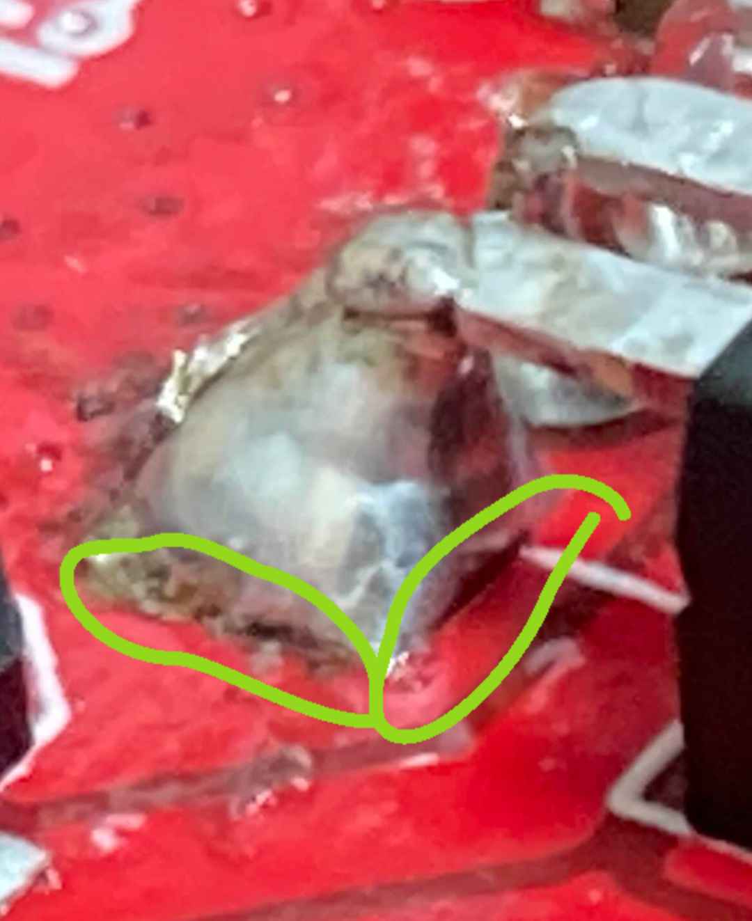
I can only find them on the chinese sites so I don't have much information on them, I do know their dimensions, they should be copper, and there is this

(The model I picked does not have that tab on the bottom)
Surface special plating Guarantee against oxidation Easy to tin
I think the flux I have is this. I will definitely use a lot of flux
i like it has a "One-word" screw 😉
...sounds like you should be ok with the hot plate+iron.
sounds good
Here is the motor driver with just the mosfet circuitry
I might clean it off now
lol
I preheated the lugs before I put the rest of the board on the hot plate, and that worked great
They immediately melted the solder paste when I plopped them on
that's good!
I think the first pin on your MOSFET is a little dry,and the third one is both a bit over-wet & looks a little strange like maybe something didn't fully bond well.
Also, just for future reference, if you're hotplate-soldering SMT components, it's highly preferred to hot-plate solder all of the SMT components before any thru-hole stuff, so there are no tht-legs sticking down & no THT holes for the solder to leak down onto the hotplate through.
That 1st pin is a bit dry, I didn’t really have a good angle to reach it with the iron but it’s good enough for now, the 3rd pin took 2 soldering irons to heat up enough to get a real bond, but a little blob was hanging off which is why it looks a bit weird
I do this already, but i needed to clip the pins flush for the heat sink and I didn’t put solder paste on those pads anyway, just the big drain tab
ok 👍
Seems like you need to heat those planes up better :D. Even when conventional soldering (more like desoldering, thats the harder part IMO), I sometimes like to hot air preheat the planes to around 100C because they just suck the heat away otherwise making soldering hard.
I swear that 1 blob looks a lot better in real life 😭
Maybe this is a better angle haha
not wanting to "poke at you" or anything, but these undercuts demonstrate "cold joint" with the solder having not fully bonded to the pad, because the pad didn't get hot enough (I have to fight this problem frequently myself).
that's what was happening before i starting using 2 soldering irons
but the shading there is from the flux
i swear 😂
i am about to start testing it
that's cool...I guess it could be flux just making it look like a shadow from undercutting.
From the other angle we can see that the solder is not molten into a single piece. Like when you add blobs from your iron.
Not trying to criticize your skills, just trying to help. As Rob said, it has happened to us as well
looking at it again, that could just be a few bits of "slag" sticking on top of the solder.
I was talking about this angle. When I'm only prototyping and it's not meant to hold up for any longer than just testing, I don't care about these on my work. It should hold up anyway

yeah,that "crust" is more visible as something attached to the outside of the solder blob in the 2nd pic...but for now, "as long as it works for testing"
When I was soldering that joint, and I got a nice blob on there, a little bit was sticking off bridging to an untended via or something, so a bit later I just tried to smooth that little imperfection out and it made it look a lot worse
Anyway the testing was going well until I tried checking the voltage, but I may have hit something accidentally with the multimeter probes and then this happened 😭
luckily my laptop that was connected to the arduino still works, and the uno still turns on
but it isn't connecting to the computer anymore 💀
KAPOW!!!
Was that a P-channel?
it was an n-channel
hmmm...must have shorted VCC to GND through it then
...the FET became your unintentional fuse.
(I asked about P-channel because they're often used in applications where the gate can VERY easily end up being over-driven).
😭
better than anything else
any ideas why my uno won't connect to my computer anymore?
the USB ports still work and I am using a different cable now
do you have a multimeter, and/or another mcu board?
ive got a multimeter
Well, you can check the voltages on various parts of your board with the multimeter while it's plugged into USB. ... how long has it been since "the incident"?
about 20 minutes
also, the only connections from the Arduino to the motor driver were GND and 5V
was it plugged into usb at the time?
yes it was
when it happened, the arduino and the computer turned off too
yikes...check the polyfuse first...you might get lucky & it saved everything.
should i check its resistance?
yes
@Taire Look at this, we like seeing that. Some juicy naked FETs 🤪
haha bin there
funnt fed does bang
it's at .7 ohms right now
not plugged in
ok, plug usb in & see if the uno is recognized.
it still isn't unfortunately
also the L and ON leds light up but not any others
yeah, hard to know a whole lot more without a second board to try bypassing the ch240
this one's got an atmega16u2, and I recently bought a fake ftdi serial adapter or whatever, so could I use that?
sure, can try hooking it to TX & RX on pins 0 & 1
...see if you can program the board that way by using the F(ake)TDI as a fake 16u2
im crossing my fingers
i got that error, but is it because i only have tx and rx connected to the board and no power?
do need 5v power too.
i connected the adapter's 5v and gnd to vin and gnd on the arduino, but now the uploading message just stays there forever
sounds like it may be time to hold a funerary ritual
🪦
😭
but don't i need to connect dtr and cts too?
only if it somehow got enough amnesia to identify as a faxmodem now?
...dunno when RTS (Ready To Send) got renamed DTS though.
lmao what
this is what I am using

RTS/CTS is for "hardware flow control" and mainly only used by old school faxmodems
what about trying to use the DTR pin too
DTR is I think the new name for RTS...I just haven't managed to figure out what some idiots decided was soo non Politically-Correct about saying "Ready To Send"
DTR prob. means something like "Data Transmission Ready" or what not
this is a piece of a schematic for a ch340g chip to an atmega328pb, and it uses RX, TX, VCC, GND, and DTR, but not RTS

ahh, interesting, can try it I guess
resp=0x30
resp=0x20
Seems like somethings happening. Not just 0x00
maybe some hope
i tried connecting dtr to the reset pin, but i might try somewhere else
maybe find where else DTR label is used in the schematic you cropped above?

so i am going to try and find somehere else on the board that would actually work as dtr
ok, wait...notice how that capacitor is wired?
yeah, that's why i figured the reset pin wouldnt work since it's on the other side of the cap
(it's an "AC pass-though" capacitor...allows the DTR pin to VERY briefly toggle the RST pin; then the 10k pullup resistor re-enables the chip)
well i found a pad i could hold the dtr wire on to, but it still didn't upload
though when I touch the dtr wire to that pad the L led blinks for a second
and when I take it off
well time to get some fake nanos 😭
do you think I would be able to buy a new atmega16u2 and replace it with the old one?
if your soldering skills are up to it...what's the lead-pitch on that one?
Afaik on the arduinos the 16u2 comes in a leadless package. So only hot air could be used
still also have to get the chip aligned with the leads properly, and get just the right amount of solder on the pads.
it probably wouldn't be too hard if i could use the hot plate, but there are too many tht leads sticking out the bottom for other components
and I don't have a hot air station unfortunately
but I do have a hot air gun....
well, wouldn't I also need to program the atmega16u2?
Try it on some old electronics and report back about the amount of smoke and delamination because of it
I wasn't contradicting you by any means. Just adding more problems to the one you listed
😂
I meant seriously haha
I believe you
but, i will need to program the atmega16u2 right?
so it can work as the converter?
yes...that's what the other set of ICSP header pins are for.
well that is definitely out of the question
i might just put the atmega328p on a breadboard with the serial converter and just use the chip that way
i think all I would need is a tht crystal with tht caps, or a tht resonator
...if u can get it to "live" that way ... will prob. want to re-flash the fuse bits to set clock rate to <=8MHz from one of the internal oscillators.
lol, we were both typing about the xtal at the same time.
the chances were high 😂
I'd use an internal oscillator over plugging a crystal into a breadboard 1000x out of 10...even if just "on principle" 🤣
I think I would feel better using an external crystal instead of flashing a new bootloader, keep it so the chip is still "arduinoy"
there are multiple internal oscillators? 😲
in the 328P
high-speed RC, low-power RC, ULP 32k WDT osc., maybe a PLL too
(feel free to fact-check me on the datasheet there, though)
plus I haven't even figured out how to flash a bootloader on a different atmega328 chip
Interesting
yep, I will look it up, don't worry 😄
and also try them. I only knew about the watchdog timer being separate
once I get some new boards, how can I protect them if this happens again
like these?
I kind of missed what happened tbh
the atmega328pb in the leadless package
...or the ATTiny 16u4 with the legs & cap soldered onto it here?
mosfet blew up, killed something with the serial converter on an arduino uno
shorted VCC to GND and popped a power MOSFET 😂
no thank you 😂
Yeah but I saw no extra components. Did you have an Arduino connected to its gate?
i had 5v from the arduino connected to the gate
and gnd connected to the gnd pin
8'd add programming pins on my PCB
:this:
big-chicka-boom
Resistors and transistors go a long way. Or if you want real isolation then,... that. Optocoupler or digital isolator
This is the board that I am trying to program an atmega328 on

Aren't those programming pins? Haha
well I wouldn't be too sure how I could wire in restistors or transistors
yeah, but I can't figure out how to use them lmao
You burn a bootloader using ICSP connection first

You need to figure the pin outs out
i had done this, connected to the arduino uno I killed today, and tried following a tutorial to use a minicore bootloader, but I kept getting errors
It seemed like i need a usbasp instead of another arduino?
ok, so I see a ch340 & a 328.... and suspiciously only 1 set of icsp "pins"?
...which it would really help to solder on actual header pins there.
yes, just for the 328pb
it would 😫
im thinking i will just use a different power supply to control the gate
Using a power supply to... control the gate? How does that work?
well i was just using 5v from the arduino before, so if I find a 5v power supply i could use that
I think i have some old barrel jack wall supplies that are 5v
Isn't a mosfet made for switching things on and off? Whats the purpose of that?
...dunno what the intent is here, but if you just need to protect the arduino, opto-isolators & digital-isolators are a thing.
the 5v would be to power the gate of the mosfet in the motor driver
And what exactly does the mosfet do? Does it ever get switched or something?
If i had an optoisolator i would use it, but I don't want to wait the time it takes to get some
i was thinking about this, but for the test I wasn't planning to use an pwm or anything, just keep the gate open
im hoping the dc wall supply could take it 😂
seems like 2 days waiting for an optoisolator delivery is better than 25 waiting for an aliexpress shipment of replacement arduino boards 😂
if i want that fast delivery though, i would have to spend $8 on opto isolators on amazon
ok, how much for that pcb, lugs, mosfet, and your time & effort assembling a new one?
well it could blow up regardless
A resistor to gate would go a long way
i might do that
but it also wouldn't be 5v going to the gate anymore
Sure about that?
no haha
what resistance would I want?
im not sure how I would calculate that
enough to not blow up the 5v adaptor with the 12v backfeeding through the resistor.
i couldn't tell ya
i think I have been convinced to get an opto isolator
😂
Your problem lies in bridging things that shouldn't be bridged. Like VCC to gate/GND/....
The opto isolator is not the solution to the problem, but in case of a problem it would save your Arduino and PC
yes and this is what im looking for
im trying to firgure out how I would use one though
for this case
Preventing the problem from happening would be a potentially better solution
would the output of the optocoupler have a significant voltage drop? NVM
also im not even sure how to wire this thing

the collector would typically go to a pullup resistor, the emitter to ground
when light hits the phototransistor the collector goes to ground, when off the collector goes to the pullup voltage, the collector voltage drives the MOSFET gate
What PWM frequency are you looking for? Above some, you will have troubles with a simple optocoupler connected to GND
i wasn't planning to use a pwm frequency
Yes, but after the testing is done?
well i haven't though about that
i haven't seen people use optocouplers when controlling mosfets
is that a normal thing?
very common between a low voltage controller side and a high voltage output side, the light beam provides high "galvanic isolation"
maybe I should add an optocoupler to this board if i make another revision?
Have you thought about switching speeds?
ah I guess that wouldn't work well with super high frequencies then
that inverts logic on the MOSFET gate though, which can latch the MOSFET "on" if the arduino loses power, no?
digital isolators work well inti the MHz range
...they just often cost a little more, and take more pins.
A transistor to amplify the output of the optocoupler could go a long way, couldn't it?
But as long as we don't know the requirements,we are just shooting in the air with our suggestions 😂
could re-invert the logic, but since the optocoupler is already using an internal transistor (or darlington pair) as its output...
I thought that those have quite an internal resistance and that they can only supply in the range of 10mA-s limiting switching speed greatly
idk, depends on the exact model.
well thanks for all the help guys
hopefully i can restart testing this again
(and be more careful with my multimeter probes)
for testing, could add some 2.54mm header-pin THT footprints to the pcb. Easy to stick a probe into one of those & not worry about it sliding around & causing shorts
i was sticking the probes into the heads of the screws on the lugs which were very stable, just very close to things i could short
yes, so was I ... with gate tied to collector, and a pullup, isn't the power N-MOS going to be "On" any time the mcu isn't activating the opto?
(or did I "do a dum" there?)
more the NPN emitter to 5v (wasn't thinking of MCU failure leaving the FET on)
ahh, ok ... I was thinking either add another transistor to re-invert the signal, or put the MOSFET gate on the emitter, with a pulldown resistor.
...but maybe I just worry about a latched-on failure too much.
for my next revision of this motor driver, I was thinking I could use a reverse voltage protection circuit like the one shown below to protect the microcontroller or whatever else is controlling the mosfet

but I am not totally sure how I would implement it
I'm working on similar circuits right now. Whats the issue?
well, i guess i would make the "load" the gate, and the "30V" the microcontroller pin output?
I'm not really following you there
i want to protect the microcontroller from anything bad on the high power side, for example a short circuit sending reverse voltage back to the microcontroller
look into translrbs and tvs diodes
they can help with shielding of the microcontroller but it does come at a cost of more parts and this more cost
wouldn't a simple digital isolator do plenty more protecting, and with only a single part?
depends on the speed they need to work at work were we have alot of esd and shorts (don't ask why we just do) and digital isolators arnt fast enough to catch those
ummm, what?!?!?!? I think we're talking different languages, because what you said roughly equates to "teeter-totters don't work for jamming SCUD missiles"
Digital isolators don't "catch" anything. They keep the two circuits entirely separate from each other. It's up to you to make sure you aren't building up enough static potential between the two isolated circuits to breach the isolation and arc-over at the closest/weakest point.
I believe, in @Patrick 's case here, the two VC domains will still be sharing a common GND connection, so there's no concern over building up the multi-kv potentials that you apparently encountered at your work.
ahh oke kinda missed that only read like half the posts
and the potential we reguarly build is in the naiberhood of 15-200 ish kv
and there the transorbs.tvs diodes are the only thing that seem to be fast enough
its more esd then what partick is experiencing i suppose
yeah, a digiiso is fast enough to transmit data faster than an optoiso...but when you have potentials that will build to hundreds of kv, you simply need "more than isolation"
yea again misread there ignore what i said
I think Patrick is only trying to protect an MCU pin from potential backfeed of a 12/24v VCC should a MOSFET fail spectacularly enough to short GATE to SOURCE.
np, was just a bit confused, since your posts usually do NOT strike me as "what is he thinking"...so I figured there had to be some kind of miscommunication happening.
gate to source is a rare one i usualy onle see source to drain
tho tbf with what i do uualy the mosfet just deletes itself from the design
xd
I think it was a "testing accident" where they multimeter probed slipped
like only thing left being the legs
posible but till a good idea to add protection to that
oh, I agree...lots of ppl use "gate resistors" with their MOSFETs & 99x out of 100 I think they're only causing themselves more problems...but in this one case, Patrick seems to have found the "magic formula" for causing a Gate-Source isolation failure AND damage something more expensive than the MOSFET upstream.
"gunshot failure" ... everybody instinctively ducks to avoid the flying transistor bits 😂
Bruh 😂
Would digital isolators be able to “switch” fast enough with a high frequency pwm signal
define high frequency
I don’t know lol, I just hope @robherc KV5ROB gets what I mean since it would be for a mosfet
they work into several MHz, and I bet more expensive ones are likely available that can top 100MHz
So that is probably something people would almost never hit?
With a pwm frequency that high
usually your pwm frequency will be under 500khz in my experience
great then, thanks!
i began testing the motor driver again today, and it was going great
but the 50A bridge rectifier on my power supply keeps over heating, and when it does it starts to smoke and makes the transformer get a lot louder. Im only at 20A too
it does still work, maybe i can run it underwater?
the bridge rectifier in question: https://www.aliexpress.us/item/3256801251045663.html?spm=a2g0o.order_list.order_list_main.50.d30e18027Y65lX&gatewayAdapt=glo2usa#nav-description

saw this lol
Weird that yours get smoking smoking hot
i am able to see a bit of smoke while its running, then when it gets too hot it immediately lets out a bunch of smoke, and keeps going until i unplug the transformer
even if there is no load anymore
it like shuts down into a thermal runaway or something lmao
Im guessing the epoxy or whatever the black stuff is, is what is burning or melting
do you think running it submerged in tap water will work?
how are you keeping it cool? I highly recommend AGAINST water immersion, and oil immersion should be approached with EXTREME CAUTION (fire hazard)
im just letting the built in heat sink handle it, but its not doing enough
maybe try some fan action next time
ive got the perfect fan for the job
@robherc KV5ROB i was thinking of trying to use optoisolators instead of digital isolators for safely controlling the mosfet gate, it seems like they support a wider range of voltages.
and It also seems like they can support a pretty high frequency pwm signal
yeah, opto's are usually a good bit slower than digiisos, but generally could be fast enough for power pwm.
just for high-speed data busses, a digiiso will likely be a better fit (obv. not needed here)
so I am not totally sure how to incorporate optocouplers into an h-bridge...

Im not really sure what to do
wow, I wasn't prepared for how ridiculous that would look to me, lol.
Anywise...your N-channel FETs are always conducting, so ghat isn't an H-bridge, it's just shorted out. Also, your P-channel MOSFETs are likely to need gate-protection zeners if their Vhs(max) is lower than your open-circuit supply voltage.
If you were going optocouplers, why not separate the grounds as well?
nothing gained there, probably.
iirc, he's just using the optos for "bulletproof isolation to backup the power MOSFET gate isolation."
Even if they are shorting VCC and GND accidentally?
Or having a ground break and the current could maybe even travel through their Arduino? Which won't be caught by the polyfuse
I know these should be avoided but in the first place he is still trying to avoid these "accidents" and the consequences of user/testing errors. In normal operation they wouldn't really need anything, right? 😂
shorting VCC to GND pops whatever component in the power train that acts as a sacrificial fuse (or circuit interrupter) first, but now he has successfully ensured that won't be his MCU chip. 😂
ofc, an avr chip costs about $0.82, while most optoisolators are over $1...even most aliexpress dev-boards cost less than putting 4 optos on the H-bridge, so it would really still be less expensive to just buy a few spare arduinos, tbj.
Lmfao
I’m going to try something else
well it definitely wasn't worth the $30 for a real arduino
and came close to killing my laptop (it seemed like)
so I think It would be worth it lol
plus the ones on LCSC are way cheaper than that
Did you completely kill it?
are you what voltage ya running at and whats the forward voltage of the diodes(if you know that value) then you can calculate how much you disapating in heat
also is it using diodes or feds for the rectifcation
Well it doesn’t connect to my computer anymore
Not completely killed though
About 20v is my vcc, don’t know anything else though
I’m pretty sure it uses diodes
well i got everything setup to restart testing the motor driver and it turns out yesterday's incident with the full bridge rectifier finally killed it
hopefully i can get my money back for that lol
I think this will be my replacement: https://www.amazon.com/Baomain-Bridge-Rectifier-MDQ-100A-Module/dp/B01JIKSHCA/ref=cm_cr_arp_d_product_top?ie=UTF8
Baomain Bridge Rectifier MDQ-100A 100A 1600V Full Wave Diode Module...
Baomain Bridge Rectifier MDQ-100A 100A 1600V Full Wave Diode Module One Phase
I could use this

and then find a way to either use a digital isolator or an opto isolator on the gates
actually, could I use a gate driver for the gate like this one? they have some hella fast speeds https://www.digikey.com/en/products/detail/infineon-technologies/1EDB7275FXUMA1/14309451
DigiKey Electronics
1EDB7275FXUMA1 | DigiKey Electronics
Order today, ships today. 1EDB7275FXUMA1 – 5.4A, 9.8A Gate Driver Magnetic Coupling 3000Vrms 1 Channel PG-DSO-8 from Infineon Technologies. Pricing and Availability on millions of electronic components from Digi-Key Electronics.
I feel like using a gate driver would be the way to go?
nevermind that they all have too high supply voltage ranges
I am looking at this digital isolator mainly: https://www.lcsc.com/product-detail/Digital-Isolators_Texas-Instruments-ISO7720DR_C486037.html
LCSC Electronics
ISO7720DR Texas Instruments Signal Isolation Devices | SOIC-8 Digit...
ISO7720DR Texas Instruments - SOIC-8 Digital Isolators Digital Isolators. Check out the in-stock pricing and datasheet for electronic components from LCSC Electronics.
i am wondering if this would work, @robherc KV5ROB

well, that's what gate drivers are made for, so I would tend to agree 😉
well, it definitely looks fast enough, lol
I would not wire it that way, though. ... maybe VCC/GND on the input, and 24v/(24v-Vgs(max) on the output
I wired the low side N mos the same way (5V drive voltage) in my design but I looked up the datasheet and it should be fine? It has a 20V+- Vgs so that's why. This is my MOSFET's graph, your has one as well that has to be considered Patrick

Also the 1k resistor on the gate slows down switching time by a lot. Completely hindering the ability of a gate driver IC. That is usually under 100ohms. Usually you also place them for each Mosfet and not 1 for the two
and you DON'T place a gate resistor at all when using a dedicated gate-driving circuit, because you're now defeating the purpose of the gate driver with redundant "safety stuff."
Well, for paralleling MOSFETs I thought it was also serving a purpose of matching them together by some few ohm resistors in 'parallel'. I'd really need to read up on that one tho
But that doesn't even matter this time
i mean that will work but seems like its jsut a tadbit overkill
assuming you dont paralell mosfets, at that point they help with matching the switching moment to redude the risk of (in a hbridge) the highside and lowside be on at the same time
but you do indeed loose switching speed at that oint and 1k is to high at that point still, your usualy more in the range of a few hunderd ohm
yes, I did mean "dedicated gate driver" to mean both "purpose-built" and "one each"
ahh yea just wanted to clarify that
otherwise ya end up with a mofed removing itself from a design rather violently
very true!
xd haha
like nothing ever happend eyy :laugh:
I think we'd all rather not know that smell 😂
what smell 😇
I wasn’t too sure about that resistor, I’ll take that off
I’m not really sure what either of you mean @KLevi
What is the input and output?
input == arduino
output == MOSFET gate
Rob is saying that feeding 5V to the driver might not be enough and that it might not turn the MOSFET completely
Ohhhh
Don’t I just need to use a voltage above the VGS(th)
Mine also have a VGS of +- 20v
this is for the n-channel

Vgs(th) is where it barely starts conducting.
yikes looking at that graph, that isn't really good lmao
Rob just saved your design. It would've blown
the p-channel one looks fine, i'll look for a different n-channel 😬
You can find a different MOSFET or get a higher drive voltage
Do you have a level shifter for the P channel?
I don't
that one conducts fine with a >=10v drive though...so where's the problem?
most development boards don't have a 10v output
you're using an isolator now, though...right?
what voltage is your load again?
yeah, but I still need to supply to it
im trying to get up to 48V
48V max
ok, so your MOSFETs are rated for at LEAST 60v Vds?
yes they are
the new ones are both 60v
So thats the max voltage on the S of the PMOS?
yes
So to get VGS = 0 (to turn the MOSFET off), you would need a voltage on Gate to be.... ?
i wouldn't know how to find that
im guessing this is something i can't do with my 5v
well, you need to drive the P-MOSFETs and N-MOSFETs separately, to avoid blowing them all up im a dead-short during switching. ...
...and you need to shift the signal-voltage from the 0-5v/0-3.3v of the mcu to the 0-Vgs(max) or the N-MOSFETs and 48-(48-Vgs(max)) of the P-MOSFETs
wouldn't they blow up anyway like my 1 did?
not if you drive them correctly
...this is where the "engineering" part of "electrical engineering" comes into play...time to get out the slide rules & scratch paper 😂
For the voltage across Vgs to be 0V, you need both of them to be 48V (or whatever voltage you want to use to run your motor)
same with like 12v?
Yes
And then if you pull the gate of your PMOS lower, let's say to 48V -10V so 38V, it will turn on
voltage is relative too
😂
so pretty much what your saying is i need to use a level shifter for any drive voltage over 5v?
yes...you want to level-shift your signal voltage to drive each of the 4 MOSFETs in your H-bridge.
well I won't need to do that for the n channel ones right?
i mean I didn't have to do it for my current motor driver board
Yes but you will still need to delay/speed up the switching times to match with the P mos...
you should do it for the N-channel ones ... they can run more efficiently that way.
quick side note what kind of motor are we driving here and what kind of current/voltage will we see
cus i was jsut adding a bunch of stuff to my parts db (dont ask) and i came across this one and it may suit your needs jsut out of the box without having to make your own hbridge
48v input 4a rms with 5a peak
5a max is multitudes too low
Well I guess I’ll do that
So I would need 48v on the gate of all 4 mosfets?
ahh fair enough never mind me then
That depends on your Vgs max
VCC to the gates of the P-MOSFETs when not "turned on"
...N-MOSFETs get GND when not "turned on" ... both get something near Vgs(max) to their gates while "turned on"
Switching that much power is not an easy task to accomplish tbh
well if i was using 48v i definitely wouldn't be trying to pull 30 or 40 amps
vgs max is +-20V for both of them, so should I just use like 18?
no, you either use a purpose-built gate driver, or you purpose-build your own, that works from the VCC that you're switching & protects the gates from any charge that's greater than Vgs(max).
Yes, this is something @Taire, myself, and several other senior EE-types here can do with little thought...but that's after SEVERAL YEARS of practice, so it's definitely no insult to be struggling with it as a beginner!
so the gate drivers don't just feed whatever vcc you gave it to the gate?
i wouldn't call myself that much of a beginner anymore
I can't answer for all gate drivers, but many even include an internal charge-pump to use the vcc to generate an even higher voltage to allow you to use N-MOSFETs for high-side switching.
i'll go back to looking for those
If you don't want separate gate drivers for the MOSFETs, then that means that 20V is the max (unsafely) that you can switch. And less with the safety margin
That's a dangerous place to be, getting overconfident while working with electronics can be deadly.
Not trying to scare you too much but ALWAYS stay alert. If you're not working with too scary stuff, just keep it in mind that at some point you will probably start working with stuff that if you do something wrong, it's the last thing you ever do.
TLDR don't get overconfident.
anyway that lout of the way
infineon has alot of very nice/confinent gatedrivers that take a voltage input and with a intergrated chargepup drive the gate of the fed
(and don't take "beginner" as an insult, unless the context makes it impossible not to...there's nothing wrong with being new; just means you're learning this stuff faster than the "old pros")
exactly ^^^
on another note what kind of feds are you using si or sic, cus in the case of sic you NEED a gate driver incase of si you can mostly get away with it
i am not really sure how these work
sorry not that one
something like this one https://www.lcsc.com/product-detail/Gate-Drivers_Infineon-Technologies-IR2104STRPBF_C2960.html
LCSC Electronics
IR2104STRPBF Infineon Technologies Motor Driver ICs | Half Bridge 2...
IR2104STRPBF Infineon Technologies - Half Bridge 2 210mA 100ns 50ns 10V~20V 360mA SOIC-8 Gate Drivers Gate Drivers. Check out the in-stock pricing and datasheet for electronic components from LCSC Electronics.
i would use 2 of them for each side, and connect the high and low mosfets to HO and LO

one of the main thing's i am wondering about is why is there only 1 input for controlling when they are on or off
do they mean "in phase" as in HO and LO get the same signals and power?
it's a "half-bridge" driver... turns one on when it turns the other off.
and it turns one on/off when i give it a signal?
yes, you signal HIGH, it turns one one & the other off...signal LOW and it turns the first one off & the other one on.
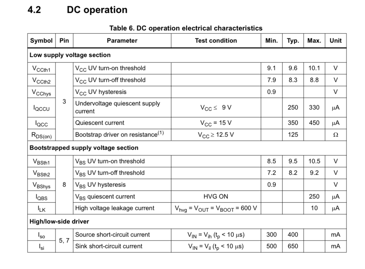
thanks, how about the vcc and vb, im not really sure how those work
vcc is rated for 10-20v
and vb is a max of 600 ish
hmmm... 10-20 does not include 5v 😕
vb & vs are powered by the load that you're switching
so the "big concern" here is the 10-20v VCC & the fact that it likely means the inputs need a minimum of 9.7v to signify HIGH.
im looking at one now with a vcc rated for 5-20v
check the input voltages for in-HIGH in the "electrical characteristics" section.
it's 0-VCC
no
...wrong line 😉
whoops
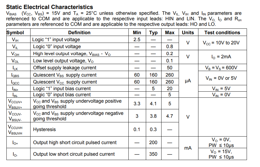
i'll just send the whole table because I wasn't sure which one you are talking about

VIH == 2.5v minimum to register as a HIGH
so that's gonna work
would I be able to make the whole h-bridge with just n channel mosfets now?
looks like that's what that gate-driver is built for, so I think so.
hooray!
i just realized, you wouldn't be able to use pwm to control the motor speed right?
how not?
Stepper-drivers use closed-loop adaptive PWM to control the current through stepper motors' coils, to +/- a few :mu:A
how would I do it?
the same way as if the transistors were attached directly to your mcu & only controlling a 5v motor.
...just check the switching speed-characteristics of both the gate-drivers and the MOSFETs.
Make sure you're not trying to switch the circuit "too fast" with your PWM signal.
but the single input I have only turns the one mosfet on and the other off right?
if i send a pwm signal through that, it would just reverse the motor super fast
yes
you have 2 sides to your H-bridge
hint: what happens if you toggle one side of a coil between VCC & GND while the other side of the coil stays connected to GND the whole time
but wouldn't the 2 pwm signals need to be synced up perfectly?
Did you read the spoilered hint?
yeah i did
im not sure how it fully corelates
use one gate driver for direction control & the other for PWM speed control.
...and the answer is the coil ends up working similar to the inductor coil in a buck smps
ohhh thanks
it's like a riddle lmao
here is the new schematic

here's the datasheet's reference design

Im guessing all the resistors on my schematic would be 10k pull downs?
i just realized that there are 2 inputs on this driver rather than 1, the HIN and LIN
does this mean I can control each mosfet by itself unlike the other one that just switches one on and the other off?

looks like it
...though pls be mindful of the body diodes when trying to "switch both off at once" 😉
I have the HIN from the first gate driver connected to the LIN of the second, and the LIN from the first driver connected to the HIN of the second, this way I can just send a pwm signal down one of those wires to get the motor going one way, and vice versa
that would work right?
what?!?!?
is your goal to blow up the gate drivers? misread...thought you were driving the secondary side with the output gate-driving signals from the first
I still can't convince myself of any possible advantages to this approach over using the internally-paired drivers with one line PWM signal & the other DIR
Some TVS diodes would look great on there IMO
..the other way uses fewer pcb traces & simpler code, so I'm completely befuddled as to the goal here.
i would keep that, but i found that those drivers are a lot more expensive than these
also I think people are more used to using motor drivers in this fashion
ahh, ok...so run these like those & just tie HIN and ~LIN together?
i can do that
(~LIN) being (inverted LIN, or the "LIN" with a line over it)
i am using "LIN"
LIN with a line over it is the same as normal LIN, but needs a low signal instead of high (active low)
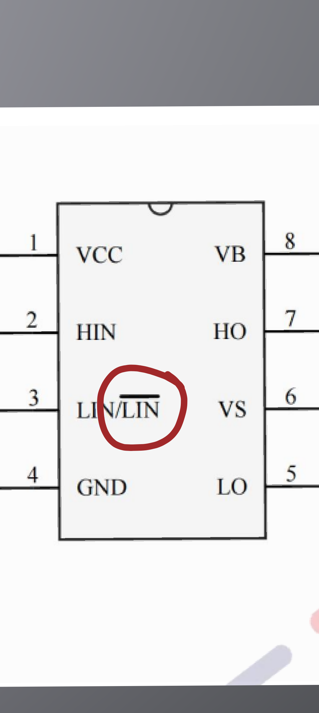
yes, so with ~LIN & HIN directly bonded as they come out of the chip.....
no sorry
the lin and hin from seperate drivers are wired together
not the lin and hin from the same driver
that's what I was saying is your problem
it's your project though, so I'll drop it now.
well it will work though?
it's cheaper, uses 2 inputs the same way other motor drivers do, and in my opinion easier to use
probably will still work...depending on exact transition-points and timing considerations...and actually, somewhat counterintuitively, I think it gives you less precise control of the motor (i.e. the pwm will be more "harsh" on the motor's coils)...but I could be missing something there, too.
now I have a TVS diode accross the motor supply VCC and GND
wait, if you're operating the mosfets exclusively tied to each other in diagonal-pairs... HOW are you PWMing at all? Inductive flybacks spiking to the moon?
(ok, well, I guess at least the body-diodes still allow some path for dissipating the spikes...but most definitely the "fast decay" current-control mode, rather than the much smoother & more energy-efficient "slow decay" schema that requires one MOSFET to still be "turned on" in the desired direction of spin.
...sorry it took me this long to come up with a way to articulate that. ... wasn't yet quite awake enough earlier.
Isn’t that how you normal control the speed of a motor?
Turn the mosfet on and off really fast
with a freewheel diode, yes...your H-bridge design you're discussing now would take away that freewheel diode & replace it with diodes that force the excess power to be shoved back into the VCC & GND rails backwards.
Basically, instead of letting your motor "coast" during the "off phase" of your PWM signal, when you operate diagonal FETs in pairs like that, you are instead forcing the motor into "regenerative braking" for the entire "off phase" of your PWM.
i see, what would be the better way to operate the mosfets
either all 4 independently, or keeping the left 2 always opposite each other & the right-2 always opposite each other (CMOS, technically)
either of those two ways, you can hold the "transistor from motor to GND" for your current direction "on", while PWM-switching the high-side FET (this allows the body-diode of the other low-side FET to act like the freewheel-diode in a single-FET pwm motor-control circuit)
It is like if you cannot turn the motor OFF, you can only reverse it's direction if I understand Rob correctly. (Didn't look into the whole thing, correct me if I'm wrong.
but to make the motor spin with all the mosfets controlled independently, I would still need to sync both diagnol pairs of mosfets to make the h-bridge work
Or just forcing GND or VCC on both sides of the motor instead of letting it float so it coasts nicely?
maybe more like "driving with one foot on the accelerator and one on the brakes" ... not QUITE "constantly toggling between forward & reverse".. but you weren't far off at all.
you would ideally do it basically the same way as I said earlier with the gate driver that always ran the HO and LO opposite of each other
though technically, if you enable both LO mosfets, or both HO mosfets, you're coasting even more efficiently than with one FET on & the other 3 off, or a single FET with a freewheel diode.
(works almost like directly soldering a wire loop to the motor, so virtually 0 back-voltage)
But in the coasting state the motor acts like a generator and at that point a very large load is connected to it. Which would slow it down faster, right?
not quite, I think...because of the switching speed mostly
Switching speed is something we haven't really discussed IIRC.
...the current through the coil is still going in the direction.that currently pulls the motor "forward" (i.e. in our desired direction of rotation), just now it's being neither pushed faster, nor pushed in the opposite direction, by any outside excitation voltage (still only during the "off phase" of the PWM control)
good point. ... because I was working from the assumption that our PWM switching speed is faster than the motor's commutation frequency.
Thanks! Also for the explanation, kind of had a gotcha' moment in there.
We don't know the application field but coasting and/or active breaking could be a design choice
it looks like almost every manufacture has their half bridge drivers always have the H mosfet opposite from the L mosfet
except for the one making the driver i was going to use
probably as a "safety thing" because if the H & L MOSFETs on one side EVER both conduct at the same time, well.....
gonna take more than Kapton tape to fix that...
Bruh 😂
I tested the driver again today with the new full bridge rectifier in the power supply, but it was still getting very hot even with a fan blowing on it, so I had to make a makeshift heat sink instead 😂

boat trailer heatsink ftw!!!! 🤣
It worked pretty well
I couldn’t tell that it was getting very hot
anyway after that one of the lugs on the motor driver fell off because the board melted the solder

At 15A the mosfet got to 117F but at 20A it jumped to 250F
do you have a solid GND plane that you can add a heatsink to on the back of that PCB?
the whole back of the pcb is flat and I bought heatsinks specifically for it
but im surprised the temperature jumped up so high with just a relatively small increase in current
check the MOSFET's curves from the datasheet
...most have an increasing resistance with increasing current, AND often increasing resistance with increasing temperature. The two of those together can cause a sudden exponential increase in temperature with a small change in current, at the right setpoint.


im not really sure how you are supposed to read that first graph
Is that 0.5 to 2 ohms on the second one?
not sure if it is ohms or milliohms
0.5x to 2x the resistance it's normallized to at "1"
so, from 1/2 to double the resistance at 25C
@Patrick that first chart is showing your max allowable current, cased on the Case temperature.
oh, so if the case is 150c I can only pass 25A
back to the h-bridge for a second, do any of these pins need to suspport up to 48V?

for example, DRVH can only output up to 38v
when it may need to go up to 48v?
if you're using 48V VCC, it is recommended to have pins BST, DRVH, & SW to be capable of withstanding 60V, from what I'm seeing in that diagram
well all of these datasheets i have looked at are all rated around 30v for those pins
maybe i am reading them wrong?
it's either ~30v ones or ~600v ones with seperate inputs for HIn and LIN
Especially if you want to use N channel high side switching.
P-MOS has to hit VCC on HO too, otherwise it would never turn off
Yep, I just that 60-48V = 12V is kind of an ideal gate drive voltage usually
i guess i will need to use the seperate input ones?
since I can't find any of the "good" kind with the correct parameters
should I use more transistors to make the inputs go on when the other is off and vise versa?
or find a different way
can always use independent gate-driver ICs for each FET. ... I'm sure there are non H-bridge specific gate drivers with a bit more selection.
that's not terribly hard to do, honestly.
(not exactly "child's play" by any stretch, but at least definitely doable)
this would still give me the same result though right?
one input and output for each mosfet
yes
...which just means you have to make 100% certain that you're turning one off before the other on the same side turns on.
i think the auto switch on/off for one of the drivers would be a good idea
how would you do that
i should try to figure it out myself first
may I recommend playing with layouts at https://falstad.com/circuit/circuitjs.html
ooOOooo that's pretty cool
thanks
Well i tried making a circuit with a n channel and p channel mosfet, which didn't work out too well. but i did some researching and it seems like i can use an XOR gate to get what i need
here is the link https://falstad.com/circuit/circuitjs.html?ctz=CQAgjCAMB0l3BWc0FwCwCY0HYEA4cEMElURTJyBTAWjDACgwE0QBmNgNnclbU9ZteUEBhEImLdl3YEQ-QXMpjSDALLyBPVgjBihrZSnWbFOvbMOjjAd2nc2GShwec8UBgBl77J6LzujpSUEABmAIYANgDOVOQeAEo+GAHJCNzB8pRImTASAOY+aHBFYBkeQA


is there a name for these 2 xor gates stacked on top of each other?
hmmm...not exactly what I expected you to discover on falstad, lol ... but I guess logic gates work (I was more thinking resistor+mosfet signal inverter)
ofc, you could also use a NOT gate if you only want to make sure both aren't ever on at the same time.
do you think the logic gates are a better idea?
they're a more "manufactured" solution...but either way should work. Whatever you're comfortable with.
alright well thanks
i guess i will do it with the XOR gates then
I've noticed on all these 4 channel XOR logic gates (not sure if it's with others too) that there is a low level output voltage of 50mV

does it mean the output of one of the gates at a low state would be outputing 50mV?
usually means if you have a pullup resistor on the line supplying xx mA of current, the output will pull the line down to no higher than 50mV above GND
ah okay, so I shouldn't have to worry about that
thank you
i just realized, do I even need to use these logic gates, if i instead use the gate drivers with the HIN and LIN with a line on top?

If I connect both inputs to the same wire, when I send a high signal the bottom will turn off and the top will turn on, and when I send a low signal the top will turn off and the bottom will turn on, right?
Worth checking the datasheet's description to be sure the HO will switch off at a higher threshold than it takes to turn LO on
but LO should only turn on if the voltage is 0, right?
or is that somewhat what I should be checking for
yeah, something to check for
I couldn't find anything for it, but i'll just post this chart here if I missed something

ok, it seems to be claiming that they have identical switching points, which should make them safe to run both from a si gle MCU pin.
Alright thank you
Here is my current design


i am using open traces on the front to add solder on top of, or solder solid core wire to, for more current
and I have a bunch of vias under the mosfets to transfer heat through the board better
I also made sure to leave the bottom side under the mosfets blank so I could put a large heatsink there and/or ontop of the mosfet bodies
I'd get rid of the vias on your output pads...looks like problems to me. Put whatever vias you choose to use outside of the area where you plan to be soldering...and honestly, I'd soldermask most of that top, a layer of solder across it will mainly just make clean soldering really hard, without much meaningful improvement.
I think "tented vias" would be find for attaching a heatsink directly over the soldermask.
thank you, I'll remove those vias on the output terminals, but I might still keep the open tracks on the top
maybe I can put some thin soldermask "barriers" to make soldering easier
Soldering on the wires will be near impossible
I’m reflow soldering lugs like the old design so as long as they don’t slide around while soldering I should be fine
Ah I see what you mean
I could put some extra wire on all the open tracks while reflowing if I did want to do that
I had an idea
Do you think when the 12v back feeeded through the arduino, it put the REAL 😂 ATmega16u2 into high voltage programming mode and erased the code that was on it?
If that was the case I could try re-programming it with whatever serial to usb code it had?
apparently the ide comes with a hex file for the code on it, so I may try flashing it
idk...thought the 16u2s were significantly older than the chips Microchip started putting UPDI HV-programming on 🤷♂️
well i wouldn't know, im not even sure if that could happen
but I might try it anyway
I am double checking that I am using the right bootstrap capacitor
I took the input capacitance which was 4130pF and multiplied it by 10 to get 41.3nF, and I rounded up to the nearest capacitor value which was 47nF. Does this seem like it would work fine?


I have been testing the new motor driver and I have one big problem. I can't switch the high side mosfets on, only the low side ones
Im not sure if I should try using larger bootstrap capacitors
high side are P channel?
they are N channel
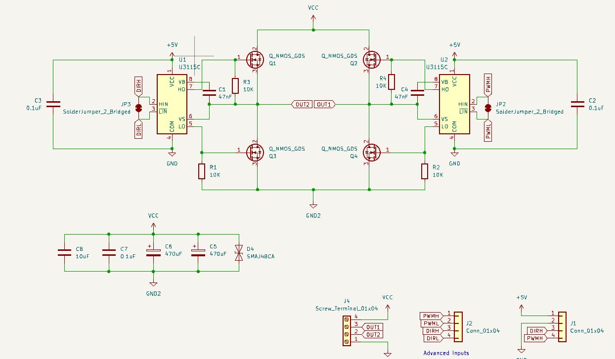
this is the typical connection circuit for each gate driver where both mosfets are N channel
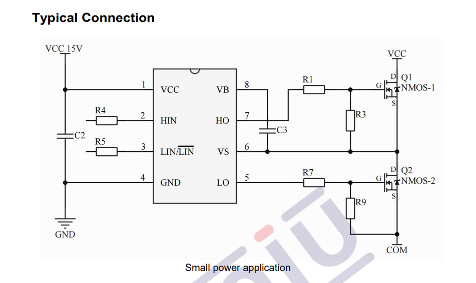
not familiar with that chip, usually an H bridge has P channels on the high side, the datasheet shows a 10uF on bootstrap
https://www.lcsc.com/datasheet/lcsc_datasheet_2409301444_UNI-SEMIC-U3115S_C400130.pdf, but again, i'm not familiar with it
that is a slightly different part, but yeah I can totally try 10uF capacitors, I don't know why they have no values on that datasheet that I was looking at
other half bridge gate drivers I was looking at from STM and Infineon also show N channel mosfets on the high and low side, so that part should be right at least
well unfortunately the 10uf bootstrap capacitors did not fix it
is there something else I might be able to test
Lol I started at the top and scrolling down and you have a high side and low side mosfet gate driver now and are dealing with the bootstrap capacitor 😂. Quite the feat considering you started only knowing about a 10k resistor to gnd.
This schematic is wrong.

No gate resistor. The mosfet gates need current limiting and maybe also a diode for the turn off.
what I am working on now is a whole different design/board than what was at the beginning of this thread, I mostly know what I am doing but I have never used these sketchy gate drivers or any gate drivers for that matter before
I can see why you would think that though, the first post message wasn't very in depth
I contemplated adding them from the beginning but it didn't seem necessary from what other people said and what I had done before
Im not sure if I would go through the work of adding them on now though since I know the gate drivers can "turn on" at least some of the MOSFETs
same deal for the diodes, I want to worry about turning on the MOSFETs before worrying about turning them off haha
Have you tried... measuring the voltages?
I wasn't sure what to even be looking for
also I watched a video on how bootstrap capacitors work, and it seems like I would need to have this diode always, even though in some of their circuit designs its not there
What voltage should the gate of the high side N chan mosfet see to turn on?
unfortunately this did not work
something like 17V, but right now when I try to turn on the high side fets I am getting about 6.5V which slowly drops
and it immediately falls to 0 when I try to hook up a load to it
Yes I am aware. This is a whole different thing. You started dipping your toes into the shallow end and ended up jumping head first into the deep end. Mosfet gates need turn on resistors at least any gate driver Ics I have used needs one. Although it looks live VCC is 5v so you are using logic level mosfets?
I have built a lot of mosfet power inverters but I typically use a gate drive transformer for very specific situations or just only work with low side mosfets and center tapped transformers. I actually am working on nearly the same project on my desk at home. I ended up getting caught up on the bootstrap capacitor as well. My gate driver didn’t have dead-time so I was using a inverting schmitt trigger, nand-gate and another logic gate to create a dead time and then I got called off to another state for work.
This is getting too long to be helpful but the 10k resistor from gate source is not needed with gate driver ics.
I know is getting long and I have not been catching up on sleep. This is a weird gate driver Ic. Typically I copy the data-sheet verbatim and work from there. Have you tried plagiarizing the example circuit on the data-sheet with no differences?
nope fets do in fact not
there are time for example when paralelling them they are needed but on a gat driver you dont get gate resistirs
With a low enough driver impedance/resistance you can get several amps that are flowing to and from the gate which can be bad in some cases
And the driver might not be rated for it
https://www.infineon.com/dgdl/Infineon-2EDL8X2X-DataSheet-v01_00-EN.pdf?fileId=8ac78c8c82ce566401837ff6a7de184a fist driver i grabed from the web
alot of the newer style and not the no name once dont require it anymore
and even if its a no name its generaly oke to not use them then either
* i will say that this is generaly on done for high switching speeds of say 250khz and above reason for this being is that the resistor (and bootstrap cap) limit the max frequency and duty cycle posible
That original motor driver project was not my first time touching electronics, I wanted to make a professional motor driver then so I asked some professionals for advice
And yes, the mosfets are fully enhanced at 5V
And I was mostly following this diagram @yourboi8500 but the problem there is they don’t state any values
I might give up on these gate drivers I am using right now and go for a more trusted brand
Could it be thst this small power application is only for when the "VCC-s" are equal, or the drive voltage maybe even lower?
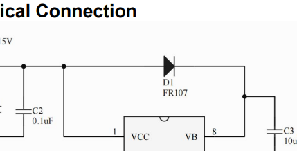
And that diode seems like the diode for the bootstrapping circuit, so soldering that externally shouldn't be that hard. Could you try that?
that must be what they mean
and I did try adding the bootstrap diodes, but it only made the gate driver high side outputs to 6.5ish volts
Well it should be integrated...
I'd look at it with an oscilloscope. Also did you try running it with some kind if actual load when testing?
I wonder why they have it on the other 2 connection diagrams then
I was hooking up a motor to the motor driver's outputs to see if those high side mosfets were doing anything, which they weren't at all
unfortunately I don't have an oscilloscope yet though
It states all the values what do you mean?
Do you not know engineering notation? 1Mhom= 1,000,000Ohms 1Kohm= 1,000 ohms.
It might be different because you are using logic level mosfets and the source voltage but it may work as a baseline. It’s like the directions on the popcorn bag the factory at least tried it once. Maybe you can start running the circuit at 12-15v like the data sheet schematic uses for testing.
I repair multi-megawatt power inverters that have their own substation.
Lol

I still think you should plagiarize the data-sheet. Don’t use the much Big POWER application schematic with the BJT’s. Use the normal one.
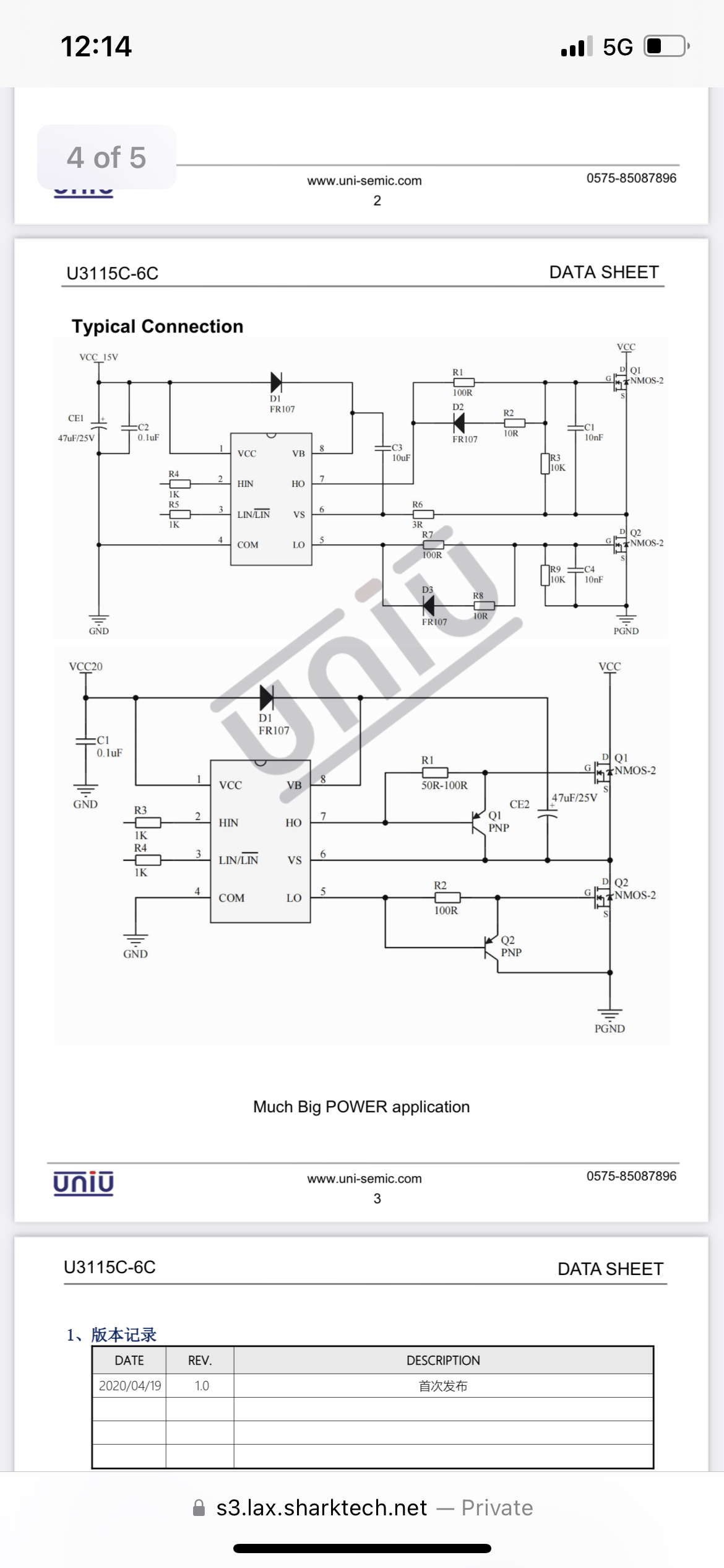
not in this one, which was the datasheet linked to the product page https://www.lcsc.com/datasheet/lcsc_datasheet_2410121731_UNI-SEMIC-U3115C_C19193019.pdf
U3115C | Datasheet | UNI-SEMIC | LCSC Electronics
Free download the datasheet for U3115C from UNI-SEMIC.
I search around for different data sheets sometimes. Different manufacturers make the same parts. Some have trash data sheets some have super useful data sheets. The one I found seems like a godsend for your application.
Sometimes it’s like TTL vs CMOS vs different package sizes. For your application any data-sheet should do the trick.
Type “u3115c datasheet” into google. With cheap Chinese crap I typically look around at a few data sheets because they have different translations or some data sheets are useless like the one your parts supplier provided.
i wonder if the one on unisemic's site is a updated datasheet, and that's why it has less connection diagrams but has the values
I might try copying their typical connection diagram then
I'm coming back to this project, and I would like to use a gate driver like this one: https://www.lcsc.com/product-detail/C2960.html?s_z=n_ir2104 The problem is, it says it has a "Gate drive supply range from 10 to 20V" but on the absolute maximum ratings chart, it can be 0-25V.
LCSC Electronics
IR2104STRPBF | Infineon | Price | In Stock | LCSC Electronics
IR2104STRPBF by Infineon - In-stock components at LCSC. Price from $0.2228. Free access IR2104STRPBF datasheet, Package, pinout diagrams, and BOM tools.
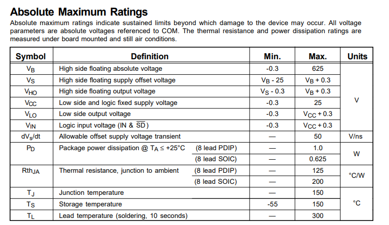
Im not sure if it would work with a 5V logic suppy voltage, along with 5V logic
What is the point of using a gate driver if you are just going to use 5v to drive the gate?
because I need to also be able to drive the high side gates
Well this will not work in my opinion
The using 5V part, or everything?
5v for logic seems fine not for driving the actual mosfets
I might add a boost converter circuit then for the gate drivers
do they not have a integrated charge pump?
Like bootstrap capacitor?
nono i mean the cirquit that generates the gigher voltage used to switch the gates basicaly theres alot of fed drivers you feed with say 15v bu they gate pin duns at much much higher voltage
the boot strap is just there to bias the high side fed
nvm looking at the ic it does have a chargepump al be it not mentioned clearly i will say that id probbly feed it with 15v to make it do a little bit less work
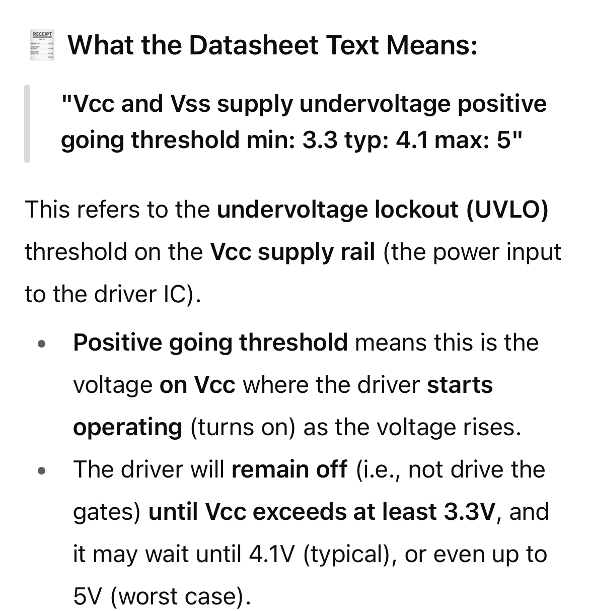
I sorta decided to just use a different gate driver with 5V in the recommended range, the only downside is that I need 2 inverter gates as there are 2 separate pins for turning on the high and low mosfets
Both active high
But if I did do it the other way I would do what you said with boosting to 15v
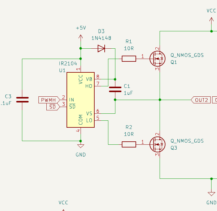
Here is the new circuit
I'm definitely not trying to do open traces for the high power lines this time
I also made sure there was plenty of space for a heatsink on the bottom and/or on the top of the mosfet body's
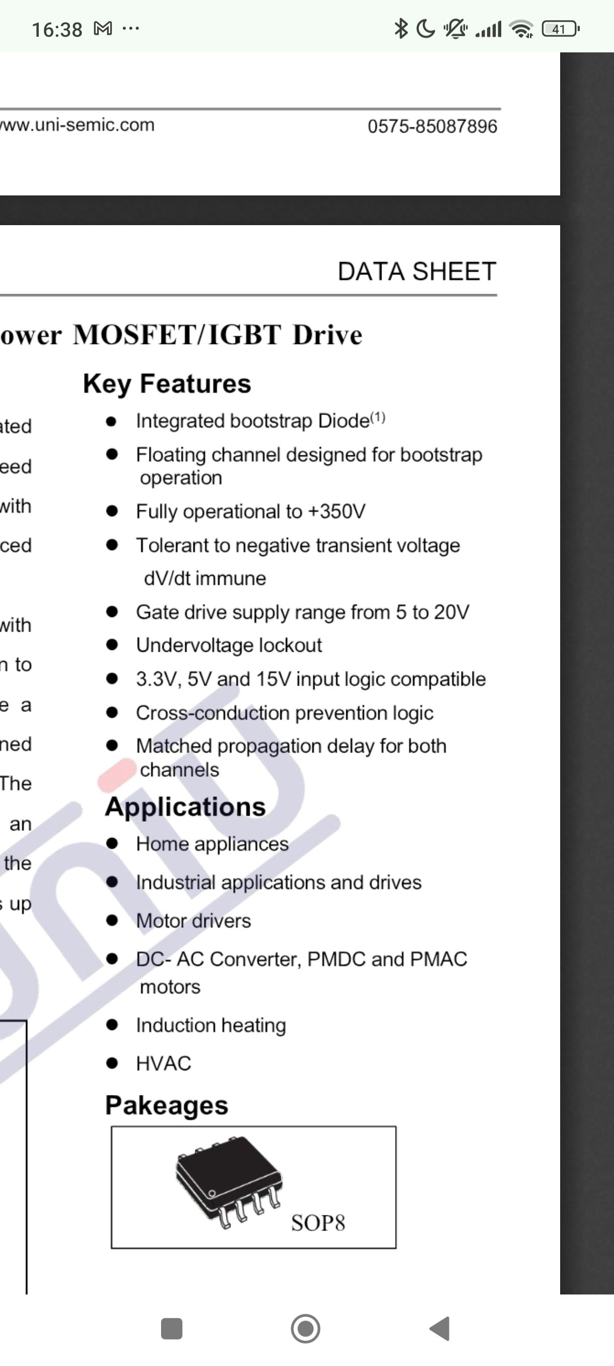
The under-voltage lock out shuts off the chip below 8v VCC correct?
Otherwise, no heatsinks on the mosfets. Usually special aluminum board is used for high wattage applications. I don’t know what you can get away with because mosfets are very efficient with gate driver ics.
I think this design is great. I would scrap the logic level mosfets and just go with normal ones at this point. But I’m assuming the motor you are driving needs 5v.
I just read your post a little closer. I see you plan to potentially mount heatsinks with thermal glue or something.
Dang, I wish I knew that before
I am trying to get everything to work with 5V, so I guess I will need to find another gate driver
I don't know if I will use any heatsinks or not, I just made sure there is space if I wanted to use one
I think I found a better replacement: https://www.lcsc.com/product-detail/C520632.html
LCSC Electronics
IRS2301STRPBF | Infineon | Price | In Stock | LCSC Electronics
IRS2301STRPBF by Infineon - In-stock components at LCSC. Price from $0.2957. Free access IRS2301STRPBF datasheet, Package, pinout diagrams, and BOM tools.
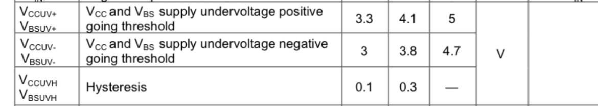
UVLO is 3.3V-5V
I asked chatgpt because it is worded strangely. I wasn’t sure if I was misreading the datasheet.
Yeah, I’m just looking for 5V so it should be fine
I think it also applies to the high side bootstrap capacitor voltage. It’s out of my area of expertise.
that should always be over 5V too
well here is the now final circuit for the gate driver stuff, made sure to add the needed bootstrap diodes
Again, it’s impressive how far you have come.
If it doesn’t work at 5V try 12V as the first troubleshooting step.
Mosfets would need to be changed to 12V gate also.
Decoupling .1uF is on the low end.
UVLO is still marginal.
Actually with UVLO being marginal close to the VCC supply voltage decoupling should be larger than normal. Logically.
I really did know a lot of this already when I was making the original
I think it’ll be fine
The very max was 5V and the datasheet had a lot of references to 5v compatible vcc/logic
Here is the new version assembled, just without the big caps for now until I know it works
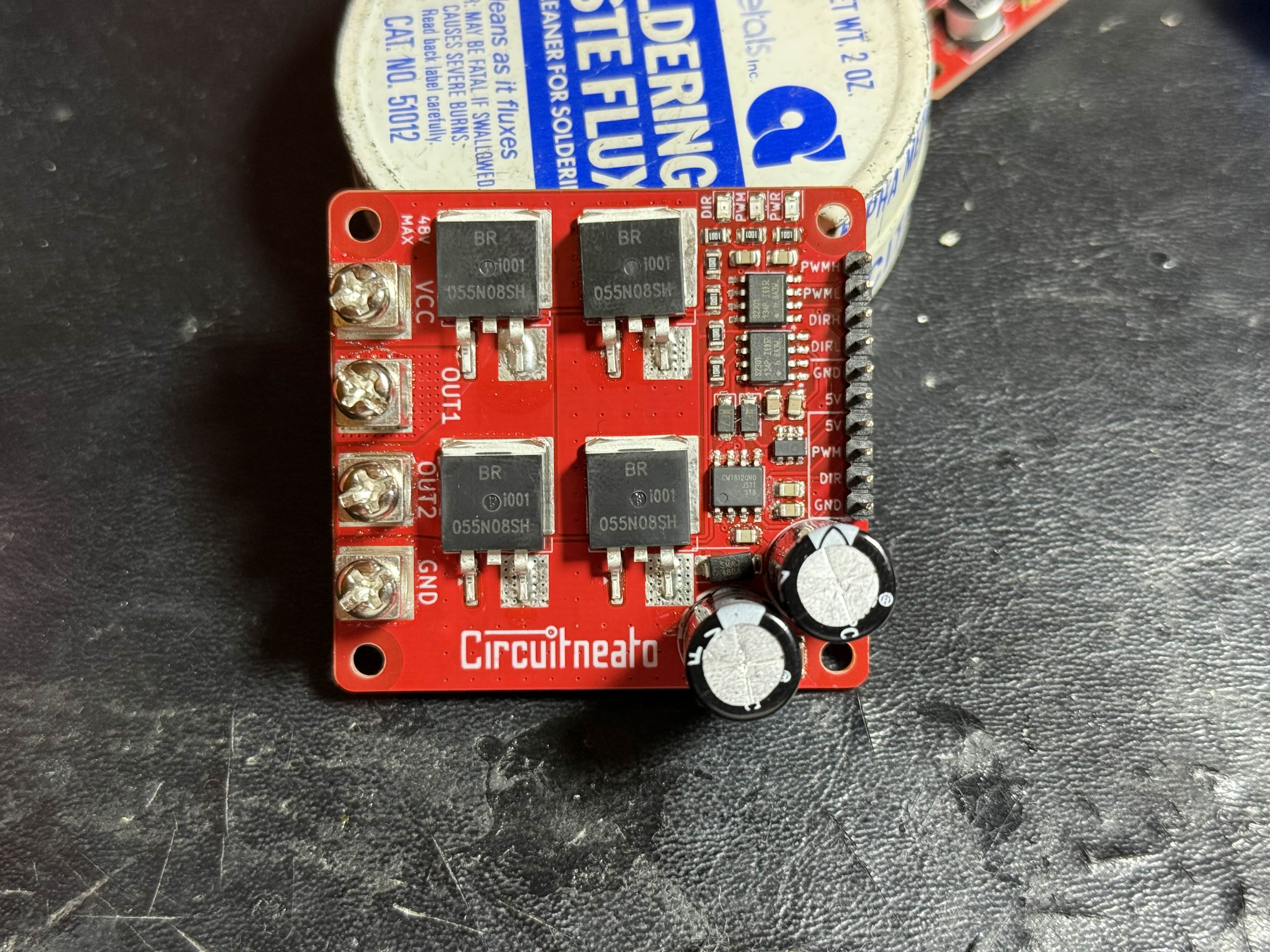
Now I need to see if it can turn on the high side mosfets, as the last version couldn’t, then I can test the max current with and without a heatsink
Noice
What a nice project, I wish I saw it sooner. Can you say why those mosfets/drivers? Is it because of cost?
Btw it is neato indeedo. I see the small vias everywhere even the "i"
The mosfets were mostly just what was available and low cost, and the drivers because they were the only ones that had all the parameters I need
Like working at 5V (hopefully)
They still weren’t perfect though
Cool! Have you tested yet? Its never 100% perfect. Look for good enough, safe enough, reliable enough... Sometimes its a matter of limiting the operation.
Also now you have a way better knowledge on this matter, and maybe you can change some parameters... Working with well known parts (even if they are not exactly what you want, say, more than 5V) sometimes is better.
Not yet
I just finished testing for functionality and it works great! I can get an over 99% duty cycle with Arduino's standard analogWrite function (analogWrite(motorPin, 254);) And 0V to 48V just fine
I'll get my testing jig set up again for this, I'm hoping for at least 40A continuous with a heatsink, and at least 20A or 25A without
passive or forced air heatsink?
i'll try passive first
fair fair
Started testing today!
unfortunately the results testing it's max power without a heatsink weren't as great as I hoped. The body of the mosfet would get up to 130C way too often, and at pretty low loads. The lowest I tested was 9A at 9.6V and it took about 30 seconds to get too hot. The max temp for the mosfets is 150C, but I didn't want to go over 130C to avoid the solder from melting.
which I think is odd because back when I was using a single mosfet, I was able to draw 15A continuous without overheating
Datasheet - LCSC Electronics
Free download the datasheet for IRLB8721PBF from Infineon.
Datasheet - LCSC Electronics
Free download the datasheet for BRCS055N08SHBD from BLUE ROCKET.
the first link is the single mosfet in the old design, and the second link is for the new mosfets in the newer design. the new ones have a higher power dissipation, lower RDS, higher max current, higher max voltage, and lower gate resistance. Is there something I'm missing?
Measure the voltage drop across the top vs bottom mosfets across your bridge for both sides and type here the information so everyone can see that an h bridge with all n channel is a bad idea even with an awesome gate driver. Im betting all in on that. Tell me if I won 😅
Also why didn't you prototype it before building the board, you seem that you also went all in.
what do you mean exactly? do you think there is a large voltage drop from the high and low side mosfets?
Btw I'm not discouraging you, Im actually really excited to help you on this one.
why wait for all the smd parts to come, put them all on dip adapters, then make the circuit by hand if I could just put everything on a PCB for 1 extra dollar, and save time if it does work first try, (which this is technically the second)
though this makes me think, maybe the pwm duty cycle isn't enough to allow the high side gates to be fully enhanced at 5V from the bootstrap capacitor
No I don't think, I sure there is. That's the only reason why a mosfet heat up. It's conduction loss and switching loss. If you are not changing pwm frequency but you keep watching a rise in temperature, it's probably a conduction loss because the high side mosfet on each branch have a higher drop for it to work, so it automatically dissipates more power even for the same rdon. Now if you see an increase in temperature for an increase or change in pwm frequency it means you have switching loss and then you have to upgrade your drive with more current, speed and a snubber.
That's why haha. Trouble shooting time. But I'm impressed it's so cheap for you. I would probably do the same knowing this. But the bad part comes now... "why and how to fix it" I built a driver with off the shelf parts during the crisis just to be sure it would work before I went and manufacture it. But it was also because of price and time to manufacture.
You can only be sure measuring it. You can fix frequency and write down voltage drop across all rdson but You will need to have an oscilloscope for this project.
I should be able to see a significant difference between the voltage on the drain and the voltage on the source for the high side mosfet getting switched then right?
Absolutely
Also compare that with all drops on all mosfets and type here. Also write the frequency and duty cycle you are using at that moment, and voltage on your load too. You can do this all with a multimeter. But again get an oscilloscope.
Now, I don't know if you will be able to do it quick and I don't want to rush you. I'm going to bed. Take your time an be sure of the measurings, I can help you tomorrow 👌
im not sure when I can set the testing rig up again, so it will probably be a while
Ping me when you do. Find an oscilloscope, also. I want to see it.
Wouldn't it be fine to calculate the conduction and switching losses?
I did, and the conduction loss is only approximately 0.6W, and the switching loss is next to nothing
Calculating again wont help you most certainly already did it. And what a surprise: They look good.
I asked about prototyping it first because of this. Going to the very basics you are missing the most important part. When combined on the circuit the voltage drops changes, because for the high branch you will have the lower fet Vds + the load voltage on your high fet source pin, that wont look good because you will need a more positive gate on high fets than on bottom fets just to have enough voltage to get to that Rdson. Thats conduction loss. Also it takes time for the MOSFET to reach that optimal conduction that gives you 0.6W. Thats switching losses. Adding to that, you need to block the lower ones on the same branch completely before switching on the top ones to avoid shoot-through and vice-versa, and before you say "but my driver does that" I'm pretty sure it is not doing it properly, and some are turning one a little before the others are completely off.
Thats why I said: now that you built it already, just measure it. Also show us the final circuit you have. You can also simulate it with a SPICE software if you want to get extra technical
This is the schematic for the h-bridge
There are other details in this chat too
And if you still want me to, I should be able to test the mosfet’s voltage without load, or at least with a very small load right?
Also the 0.6W was the calculated conduction loss, not the switching loss
Cool. I'd like to see the calculations then, and why you believe its only 0.6W conduction loss. I dont calculate much, I simulate first, then I build. To me, measuring with a good scope now is mandatory because I saw you are using not very well known drivers and mosfets, and you have to be sure how distant from your calculations the circuit really is. You must test it with the real load. And speaking of the real load, theres one more thing you should consider. Inductive loads. And I just saw a picture, it certainly does not look like a small motor but a huge microwave transformer. Those things are massive loads, I wouldnt expect it to simply work. Again I'm not discouraging, I'm telling you it is not that trivial and perhaps even limiting a lot the operation wont be enough for it to work as expected with all N-Chanel fets.
The transformer is the power supply for the the driver, not the load. The load is a low resistance nichrome wire shorted across the output terminals of the driver.
I used this equation to calculate the conduction loss:
Ok, stop right there, thats what I wanted to show you
I'm not math teacher. But that equation cares only for final, steady-state values. You dont know how your MOSFETS are behaving until the get to that area of steady conduction. Thats why I told you I calculate very little, simulate a lot and then I build (its just me). I find it the easier way to simulate all the transition states.
do you want to see the switching loss equation?
Sure... but I want to show you something way cooler
yes! but do you know the rise and fall times? have you measured on your frequency, on a specific load, on a specific duty cycle (it does matter)
I know their rise and fall times under their conditions
You know what the datasheet told you, yes, you right on that, but have you measured it on your circuit? I'm telling you by experience things do change. Thats why I told you about good enough, fast enough, and not perfect. Anyways, you need a scope mate. We cant go on assuming things work exactly as you calculated them. Also, your datasheets are from cheap-ass parts. If you cant measure now, try simulate them on LTSpice or some like that.
@Patrick look, this is what I believe its happening. Its way better to simulate or simple measure it than we keep guessing or calculating again.
I made these two circuits a long time ago with a friend on LTSpice. You can see the difference in power dissipated by the MOSFET with a bad driver and a good driver with a decent push-pull on the mosfet gate. Look for the red curve. Its the power dissipated on the mosfet in MY circuit. Without a propper driver, the pulse just lasts too long and everything heats like a toaster. Specially in high frequencies, dont matter the duty-cycle. With just very simple parts as PNP and NPN transistors we could make the power peak reduce from about 13us to only 202ns. Thats for the whole switch. For just the peak it lasts about 100ns. Thats more than 100x faster. On your circuit, I'm pretty sure you cant switch them fast enough, and thats all. The reason why is what is going to be the challenge to find as I said. Its probably because of your load, switching frequency and bad driver not sourcing/sinking enough current fast enough.
I hope the it's not the driver because those are the most expensive parts in the bom
and the only known brand
if you look at your switching times mosre specificaly rize and fall times those are rly high so its in the mid conduction state aka its not on nor off the "old fets" were even worse
UJ4SC075009B7S
take a look at that part from onsemie they advertize a much lower switching times so there will be less heat generated another thing you can look at is lowering your pwm dutycyle this makes it so it spends less thime in the half on off state for rn i do also agree with alex on the switching times of the gate driver hoe many A are they pushing?
will note that with that sic fed youd likely wanna switch your gatedrivers to somethign like UCC27511A
the part you sent only has slightly lower rise and fall times than the fets im using 32ns rise time compared to 28ns
I don't see how these drivers would work if they can only control the low side fets
and by "hoe many A are they pushing?" are you talking about how many amps im switching with the mosfets?
Patrick, its not about how fast they can switch. But how fast YOU can switch them. On my case that simple circuit managed 15A with no heatsink and almost no heating anywhere. One could say the datasheet is sketchy. The thing is the manufacturer writes exactly how it behaves on a very very specific test. So in reality, you will always have to measure and adjust for your use case. Thats why I asked you to measure and show us the curves with a decent scope. I'm not picky or anything, its just that it would be an endless guessing game, kinda pointless now that you already built it.
So you are very welcome to test and post all the details and pictures you want here. I'm curious about your circuit and would like to see it working 👍
to the gates
are you trying to say it shouldn't be the mosfets, but more so the gate drivers?
is there a way to estimate that
Most likely. But it doesn't mean they wont work for you. Thats what I meant with limiting operation. Also, I saw they are from IR, right? So they are quality ones. You can probably adapt your board and keep using them. But I wont speculate anymore, I want us to be sure of the problem first 👍
yes, they are from IR
would it be better to switch them at a lower frequency, but at the same duty cycle? or also lower the duty cycle to have more down time
Also, since we're here, may I ask you silly questions?
Whats the application? (The title says custom motor driver yet you are testing with a heating element as the load)
Do you need it to be DC?
Do you really need to build a custom driver?
Absolutely! If we are sure about the problem, the first suggestion would be simply lowering your frequency. The duty cycle has nothing to do with it.
I'd test it with a motor, but that means I would need a large DC motor, and I would also need to figure out a way to make it pull more or less current, which is much easier to do with just a wire
Fair enough. But do know that the final result will change again when you plug your real motor.
It mostly does need to be DC, and i'm making this driver because others are terribly expensive, like Pololu's drivers
I know there are differences
it's not necessarily supposed to be just for DC motors though
well I can try lowering the frequency then, I may also try doing the high power test again just using one of the low side mosfets alone, and with a steady 5V to it's gate. Similar to how the original single mosfet driver was tested
Thats a good test yes, but what I really wanted to see is the voltage drop on the high mosfets vs the low mosfets. And if you dont have access to a scope, schedule a test in your college or so, and do a checklist of every test you have to do there, write down every results and post here.
We really need to see the scope screen containing those curves for every branch:
Vgs
Vdson
Rise/Fall time on gate
Frequency
And then just tell us
Load power/voltage/current of your circuit
yes from the resistance of the gate and the voltage of your driver
usualy more amps you can push the quicker you can turn them on/off
I can go hook up the driver to a regular 12v power supply and check the voltage drop with a multimeter under no load right now, but when I tested for functionality a week ago with the same conditions (no load) there wasn't any voltage drop that I remembered between the supply voltage and the output voltage
Its ok, no need to, just tell us when youre done with the test I asked 👍
what voltage? the voltage for the gates of the high side fets after the bootstrap capacitor (which I wouldn't know) or the the voltage for the gates of the low side fets. Their gate resistance is approximately 1.85 ohms
that would be testing the voltage drop from the drain to the source of the high side fets
No, a complete test would be this
well I can't do the stuff that requires an oscilloscope, and I think I already know the voltage drop (which is unnoticeable) so I guess the only thing else to do is lower the frequency and see what difference that makes?
Bro, I like your project, I just can't keep guessing the problem with you... You need a proper test I'm sorry... But go ahead, I hope you can fix it 👍
I think we have some pretty good guesses already, and the tests I'm going to do should narrow that down even more
is this not part of problem solving?
it is but you don't know what is happening till you look at it with a scope here there's not rly anyway around it here
If I were to get an oscilloscope, what bandwidth would I want for this project?
50mhz covers most day to day needs
thanks
N-Channel mosfets are almost exclusively used in power inverters of all settings.
It’s difficult to say much without measurements. The last thing I was thinking about cooling and the choice of using standard PCB board instead of aluminum board.
In terms of the single mosfet circuit that sounds like an entirely different circuit driving a different motor.
The best thing to do would be to make a spice simulation and see if that checks out okay.
In terms of easiest thing to verify with test equipment would be mosfet gate-source voltages. Check for sufficient rise time and sufficient peak voltages.
If you had a simulation to compare against that seems to work okay you can keep probing components with an oscilloscope to see what is different.
Here’s what I have for the gates of the high side mosfets
About 700ns rise time for both the high and low side gates
The peak voltage for the high side gates is a little low though, should be more like 5v not 4.3v
The low side gate’s peak voltage is about 4.8V which is what it should be
also, i did these tests when there was no voltage across the drain and source, because there was some problem with the high power VCC and GND being shorted while the gate drivers are on
Rise times kind of suck. I would think the gate driver has more capabilities.
Peak voltage is 4.3V not 5?
Gate resistors are 10 ohms which is already low for a gate driver.
Oh you already said that.
Okay, your image revealed a decent amount of information. The mosfets gates are receiving somewhat acceptable rise times, gate voltage is somewhat acceptable. You did not capture 2 waveforms together to confirm no cross conduction between mosfets, that’s okay. You did not capture the output waveform. Under load (real load and or resistive dummy load) no Mosfet drain to source.
A spice simulation would reveal the most information by far. measurements a close second.
you think? wouldn't real life have the most factors already set
i can check for cross conduction, and if you mean output waveform as the source/drain pins of the mosfets, I can't do that right now
Here’s the cross conduction between the high and low side mosfets on one half of the bridge. The yellow is the low side fet and the blue is the high side fet
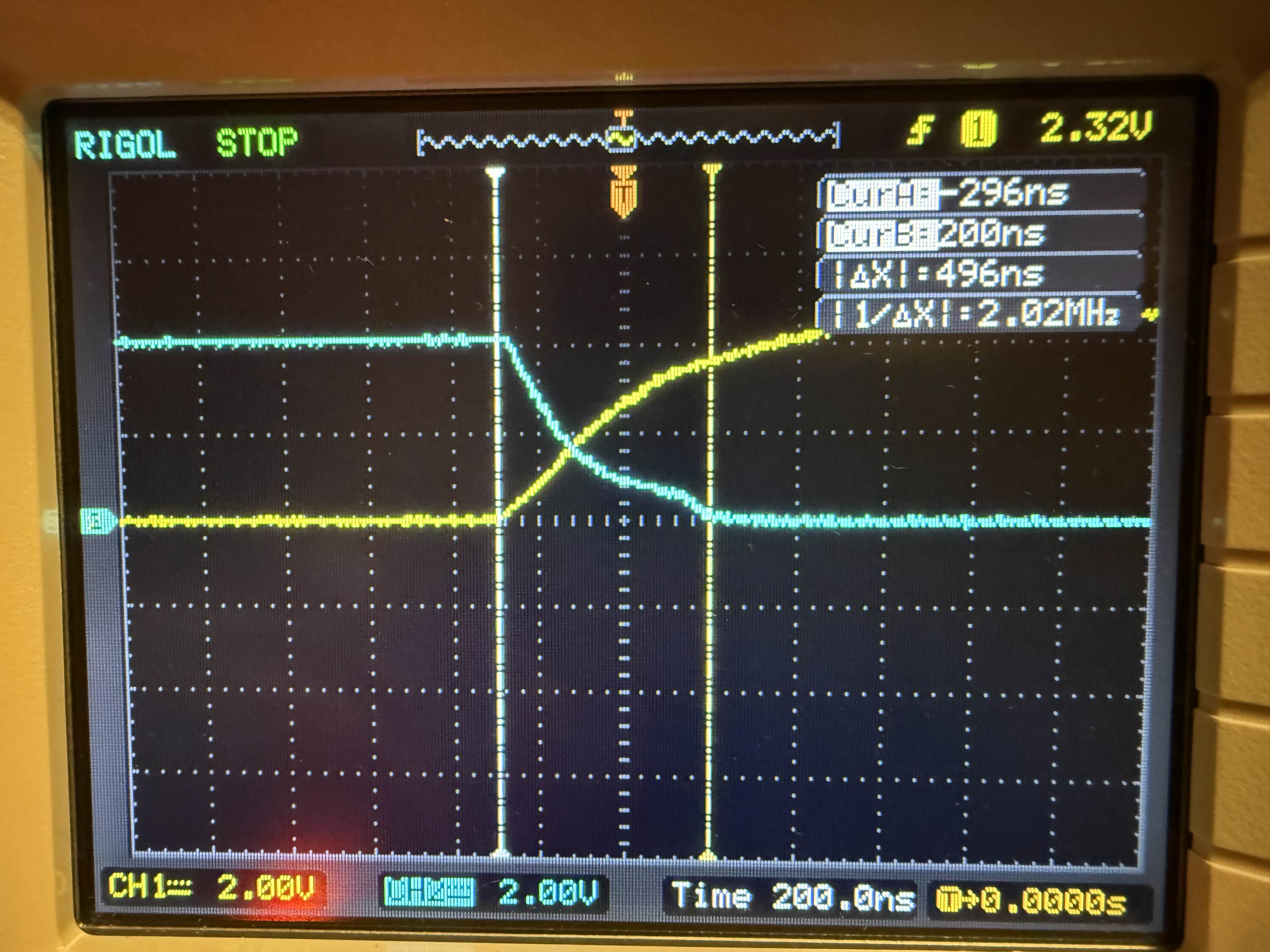
There should be no cross conduction.
Inverters need dead time between pulses.
Inverter output would be voltage over your motor. Or replace the motor with a dummy load (10ohm, 100ohm, 1k ohm resistor). Drain to source is pretty obvious.
Try introducing some dead time in the code. Even if it does not end up being the problem inverters need dead time.
This isn’t an inverter, and I’m already using a resistor as the load
There is a logic inverter that is sending the opposite signal to turn on and off the bottom mosfets, so that each of those inputs can be tied together
I've actually been looking at different fets and different, cheaper, proven, and much better overall gate drivers, so i might scrap this version for now
regardless of whether they turn on or off at the same time you need deadtime inbetween typically
otherwise they will basically short out for a fraction of a second
not sure what issue you are facing but you ideally want to avoid having any cross conduction if possible
yeah I could try individually controlling the inputs without the logic inverters, but I might just go ahead and make the new design
you can add delays to logic inverters with some simple rc networks
This is a standard H-bridge inverter. Motor drive is an application of an inverter. You are probably thinking of an inverter module with integrated voltage boosting for mains right?
If you are using an inverting schmitt trigger, not logic gate. To invert the signal you are not introducing a dead time.
Im thinking of an inverter to make smooth AC power
Square wave inverter.
Inverter is a more broad term of a circuit to flip polarities.
Really I wouldn't want to be fast switching the mosfets at all, it's just the downside of using the gate drivers
Take off the load resistor and see if it gets hot on its own. That would resolve if there are any issues with cross-conduction. If there is no load there should be no heat produced by the mosfets. Final design should have an integrated dead-time regardless of if this has anything to do with the overheating right now. Easiest way would be in the code if you are using a Arduino.
when I tested for functionality originally, I wasn't having a problem with the mosfets heating up just with power connected and them switching, so cross conduction probably isn't the main issue. also given that both fets are on for less than 500ns each cycle, not even fully enhanced
I see.
I shouldn't have this problem next version, as im using one full bridge gate driver and it has its own logic to control the fets, so I just need to send a signal for enabling the bridge and the direction
Patrick to address a comment you made earlier. Switching speed of mosfets is directly proportional to heat produced. The on resistance of modern mosfets is negligible in the case of good gate drive design and hard switching applications.
I still believe it may be worth desoldering the logic level mosfets and putting in standard mosfets and raising the circuit voltage to see if the switching speeds improve. My thought process is the gate driver is intended for 12V, the 4.3V you are seeing on the high side might be from internal voltage drops. On 12V 0.7V would be 11.3V on the gate accounting for a 5.8% peak voltage loss. At 5V 4.3V is A 14% voltage loss. The biggest part in that is If switching speeds go from 680uS to something like 340uS. I would think the switching losses would nearly half in that scenario. My concern is that the gate driver says it can output 5V on the datasheet but this might not be necessary true in the context of ideal circuit board design. This may end up costing unnecessary time, however.
My knowledge on logic level mosfets is limited. I have never really touched them. I am not much help here. A datasheet should help the people lurking on this thread. I’m not sure if you listed it above.
I came up with some ideas:
Desoldering the gate resistor and replacing it with a jumper with the logic level Fet might be a destructive test you can do. Might be able to try something like 1-2 ohms.
Also the bootstrap capacitor is directly responsible for maintaining the high side voltage. If the capacitor is too large or too small it can cause the high side voltage to drop too low. You can try raising or lowering the capacitor value.
You can measure the bootstrap capacitor voltage with the scope to see how it behaves. That’s a good point to test.
You are at the point that I am at with my H-bridge. I was getting to the bootstrap capacitor values. I was doing the dead time with analog RC timers but I was having problems with bandwidth of the input. I shelved my low power H-bridge for a few months for work has been non-stop.
My first comment may be inaccurate. 4.3V high side voltage might just be bootstrap value. Still worth seeing if rise-times improve.
Thanks for all the input, but I’m not sure if I want to spend more time getting this design to work if I know I am going to change to much better gate drivers that should fix a lot of these problems in itself
Also the rise time is only 670 nano seconds, not micro seconds but that might have just been a typo
I believe the mosfet datasheet is in the chat, but it’s probably very far up, so I can send the link again when I get to my computer. I may reuse the mosfets for the next design
Datasheet - LCSC Electronics
Free download the datasheet for BRCS055N08SHBD from BLUE ROCKET.