Bidirectional I/O buffer
For something I am making I am going to have each I/O pin of a microcontroller controlling the gate of a transistor or MOSFET. But I also want to use those I/O pins as inputs while only connecting devices to the drain or source of each transistor. Is there a type of transistor that would allow current to flow back through the body to the gate? Or would I need some extra components to do that reliably.
115 Replies
All I am really familiar with are n-channel MOSFETS
the pins going to the base of a BJT or gate of a MOSFET are outputs, not sure what you are trying to do
and if I used those pins as inputs, I would need to be able to send them a signal but from the source or drain of the mosfet
since I won't be able to reach the bare pins by themselves
the gate is an input to a MOSFET, still don't know what you are trying to do
this might make more sense

what is the drain driving? if the voltage is ok you could monitor it on a second INPUT pin, but not on the pin driving the MOSFET, which is an OUTPUT
the drain could be driving anything, it is acting as the I/O Pin but able to support more power
when it is used as an input, the mosfet wouldn't have a purpose anymore until the pin is used as an output again
as shown it's an "open drain", if can be brought LOW, but when the mosfet is off it's just floating. typically the drain is connected to a load which is in turn connected to X voltage
so forgetting about the input feature for now 😅 , Is there any way I could make something like this work? This setup with the n channel mosfet and the load on the source would need a higher VGS than normal I think?

that is "high side switching", you typically use a P-channel for that
This is what I had made earlier

see the direction of the "arrow"
though I would need the microcontroller logic to be the same as that 5V which I also wanted to avoid
you often need a driver for the switching element when you do high side

this way would allow the microcontroller logic to be lower than the VCC?
yes, a 3.3v GPIO could drive a load powered by 5 or 12v for instance
is there some other setup where I use just one transistor?
you need to be able to drive the gate up to Vcc to fully turn the P channel off
same deal with any p channel transitor?
or really any semiconductor that could work like that
yes, same with PNP BJTs
alright thank you
oh also, could I use this with 0v turning off the p channel mosfet and 5v turning it on instead of the other way around?
I should rephrase, 0V going to the transistor that then turns the p-channel mosfet off, and 5v turning it on?
for BJTs you need a current flowing base to emitter to turn it on, for MOSFETS you need a voltage source to gate
so for a p-channel with the source sitting at Vcc you need to bring the gate up to Vcc for it to turn off
but with that transistor driver, could I give it 0v to make it turn off the main mosfet and give it 5v to turn on the main mosfet?
5v to the base of the NPN will turn it on, pulling the gate of the MOSFET LOW, which will turn it on (because now there is a voltage Source to Gate)
okay good, so it already works like that
and 0v to the base of the transistor will turn the mosfet off
technically, 0v on the base causes 0 current to flow base to emitter, shutting off the NPN
since the NPN is off no current flows in the collector circuit so the gate goes HIGH
now the gate is the same voltage as the source, so no current flows Source to Drain
that's still fine right?
in the end that is what you are controlling, whether current can flow thru the load or not
And I don’t want current to flow through either if it is at 0V, so it’s right, right?
Also if I want to go back to this where the max vcc is the logic voltage
If I wanted 5v to turn it on and 0V to turn it off would I be able to use some logic gate that would flip the signal?
So when I output a high signal the mosfet turns on instead of off and vise versa
for low side switching just the NMOS will do
What would be the VGS limitations that I have heard about?
say your MOSFET needs 10v Vgs to turn on, how well will that work with an Uno pin?
that not at all 😆
is that the only limitation with high side switching compared to low side? isn't it the same either way?
sorry I got low and high side confused with each other
would it still works for high side switching, because that's what i really need
yes, Vgs is the minimum voltage you need to turn it on
so this would work right?

im confused why the current moves so slow with high side switching than with low side
no, you need a p channel
okay so back to this then, would some type of logic gate that flips the signal be the best option?
so 5v turns into 0v to turn it on and 0v turns into 5v to turn it off
if the mcu is 5v and Vcc is 5v that is a special case
you can then set a pin high enough to turn a p channel off
but i would rather it be the other way around, where that high 5v signal turns it on instead of off
which I would need something to flip the signal
digitalWrite(myPin, HIGH); or digitalWrite(myPin, LOW); 🤷♂️of course this haha, but it's more un-conventual for the high signal to be turning something off and the low signal be turning something on, at least for beginners
in any case, setting the pin HIGH will turn off the p channel, since it seems you need high side switching
I think this is what I want


when the output pin is high, the p channel turns on because of the inverter changing the signal to 0v
and the other way around
yes, if you don't want to do it in code
the NPN transistor does that very thing
i just simply wanted to flip the signal so I (or others) don't have to do it in code
right, the NPN is the inverter in your drawing
are you talking about the npn transistor here acting like the inverter
ah alright
and it becomes more general purpose because you can use higher Vcc's
I would do it like that, but it requires a lot more resistors
you only need 3
or 2
sounds more enticing
you must limit the base current to the NPN, and you need the collector resistor
let me get your opinion on this, the project is for a very beginner friendly dev board that has some of the I/O pins connected to this mosfet circuitry we have been talking about, so that people can run motors or a bunch of leds straight off the gpio pins. but do you think i should make it with the vcc being the same as the microcontroller logic, or doing as you seem to like more, with the vcc being anything and not just the microcontroller 5v logic. the downside to that it may be more confusing with so many ports for different supply voltages, im not sure if it would be that beginner friendly anymore.
the voltage needed is totally dependent on what the user decides to hook up and on the limitation of the MOSFET
what if i want to control a 12v pump?
and that's the bright side
i feel like the good would outweigh the bad
especially if i made it simple enough
i really can't say without knowing your audience
anyone new here trying to run motors off 2 I/O pins alone
you only need 1 per motor
well you know what i mean 😆
afraid i still don't, this is where we started
that was somewhat irrelevant anyways
this might be a better explanation
I am making a dev board like an Arduino UNO, but each gpio pin can output a 1A or so. And I am allowing those pins to output up to 1A by using these mosfets to switch power
so when you would normally set an output high on your board, it will set the output high on this board but just more available power
you have a 20A power supply?
I was just throwing 1A out there as a number, it probably wouldn't actually be that high
that x 20 pins...
well do you get the concept 😅
you'll need to be able to deliver enough power is all i'm saying
or you're depending on these beginners to supply external power?
I realized now I will also need a different mosfet setup to work the same way as a output pin
they are push pull
good luck with it, gtg
this is the new design

thanks a lot for your help
as usual haha
hopefully I will have enough space for all of these output buffers
Now I need to figure out how to bypass all of this to use the gpio pins as inputs
I was thinking I could use some logic gates that tell when the pin is being used as an input and change this signal on the microcontroller side, but it never worked
here's how Atmel does it 😉

Haha

It seems like that turns off the pull up resistor for the input
And is this the output buffer below?

that is how they configure the pin GPIO
Ohhhh
INPUT, OUTPUT, INPUT_PULLUP
Where are the input and output buffers
you circled the tri-state output buffer, input is on the bottom

So that is the input buffer?
yes, and the rest is the logic necessary to set the pinMode
Ah okay thanks
Also, did you say this to the first image
Or to this one
that is the circuitry connected to each GPIO pin
gotcha, then which is the one that configures Input, output, or input_pullup?
That’s an explanation of it?
as nis said, yes, that whole thing is what configures each pin
which datasheet are you guys looking at, because mine has everything in a different order https://ww1.microchip.com/downloads/en/DeviceDoc/ATmega48A-PA-88A-PA-168A-PA-328-P-DS-DS40002061B.pdf
I did find the general digital i/o diagram though.
and let me get this straight, this only connects the pull up resistor
this is just the input buffer
and im still not sure what this is
it is how the chip sets the pin to
INPUT, INPUT_PULLUP, or OUTPUT, it does all of those thingsalright thanks, i wasn't sure what you were replying to the first time
could you explain how it sets the pin to the different states?
the logic gates read the various "W" states and based on that the pin behaves differently
what is "W"?

those registers are set with the
pinMode statement
which is all to say this is not as trivial as you might have imaginedyes haha
im still confused how that buffer alone could change to the different modes, i can see how the input pullup would be triggered, but not changing the needed circuitry from input to output
I also don’t know what the “pinout” of that buffer is compared to the buffer in my circuit
My question there being what are the output and input lines for that symbol
if you look along the "data bus" line ALL those signals are generated inside the mcu and toggle the logic as needed, enabling / disabling the input and output buffers
on the far left is the pin in question, of which there are 20 on the 328 DIP package
and that diagram is a "block diagram", it isn't showing all the components needed, just the general idea of how the pin mode is changed
the circuit you were making last night is this part
that makes more sense than just the symbol above being the thing that changes it
and I do understand this, but all the lines connecting to the symbol have to mean something, and I don't know what they mean
for example, is the top line coming out of it enable the buffer or something similar?
If I could “sense” that the pin turned into an input, I might be able to use a transistor to disable the buffer or connect a wire to bypass it
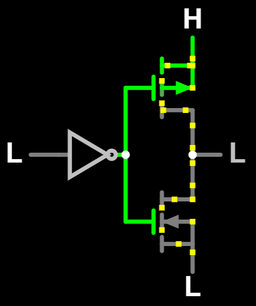
I had came up with this, but i would need a way to break that bottom connection when the pin turns into an output again

thanks for all of this, but I think i figured it out!

it works correct for outputs, inputs, and inputs with pullups!
i might use some of the protection circuits they used, but it doesn't seem like they used circuitry like mine for extra power on the I/O pins, which is probably my main feature
here is the falstad link: https://www.falstad.com/circuit/circuitjs.html?ctz=CQAgjCAMB0l3BWcMBMcUHYMGZIA4UA2ATmIxEKSshAQFMBaMMAKABkQAWPGwzm7r3xRwIAGYBDADYBnOrSgsAJrQyEQpFKvUZInEFqV1JAVykAXFgHcQPGnm4gMCLQ7yKbCNRuJa+NTQ9bOFtidTtbR0hrYJowOHdnLXjhaJsIsPsQlPdogElY0PCQzJEYKhYwBAgknz9+OpEtCqqal1s+Cga8TpotGgQYiLdC3X1ogCcuHic9ad4GgXhoji8dObWKDH7RSVl5JDSndrJ1fw7xmNq8GfPA6JVNsePXGcNjCTNLFTwwpzRkNtIu53qYLDF4kCRqVSkdIVpiJx9KU8Nh+hCwADtnFIAgdAC4Zj7GB1MwsQTKtVAa40RpCPZaX0RINWtS6QF6eymgpBgUyfZOvyNChclBoBUbELfO4pd5CQDTmzFfKBfohXgSUFfuoYZzYRiARrSZAoZqHkUudr-kyjGDLBwrdiLYQbiIIHs5ApomAZqUnfE8daytAICllstkOGQoMbH7DX8nStI4lsMbhGpRe7pJ7DjFKOt9PmXkEi88i0Wk88M7N9BEaDQPQdFBwyw0y6ldtmm0ccAWnKn++oewPCEDezXFGIKIHalX2rSwOKxZAUCwp+WZ3Mi9hsOAlzAV0MQlWB89h2cx1ugefBxPx0dzmXN5cALJdGit3jXgzilgFJ5bm2cz1kugxAA
though the new downside is that the user can't change the output voltage anymore and it has to be the same as the logic voltage, because of the circuitry for using it as an input
I also realized I could cut one diode out

well I also just realized I could do this to get the same affect, still not sure about the different vcc's though.

I was thinking, if I could use something to detect a lower voltage on the right side, then I could switch off one of the buffers, is there something I could do that with?
scratch that because it would have to be either a high or a low signal to get it to the other side
tbh, I'm not sure what I'm looking at here
without access to the registers you'd need switches to configure each pin manually, not beginner friendly at all
Im not even sure if I should use this or not anymore for the digital I/O outputs, since I am not able to use it for the analog I/O