Anas - @Seve polygon pcb smtpads not drown in c...
@Seve polygon pcb smtpads not drown in core using toMatchPcbSnapshot
51 Replies
We probably need circuit to svg support
GitHub
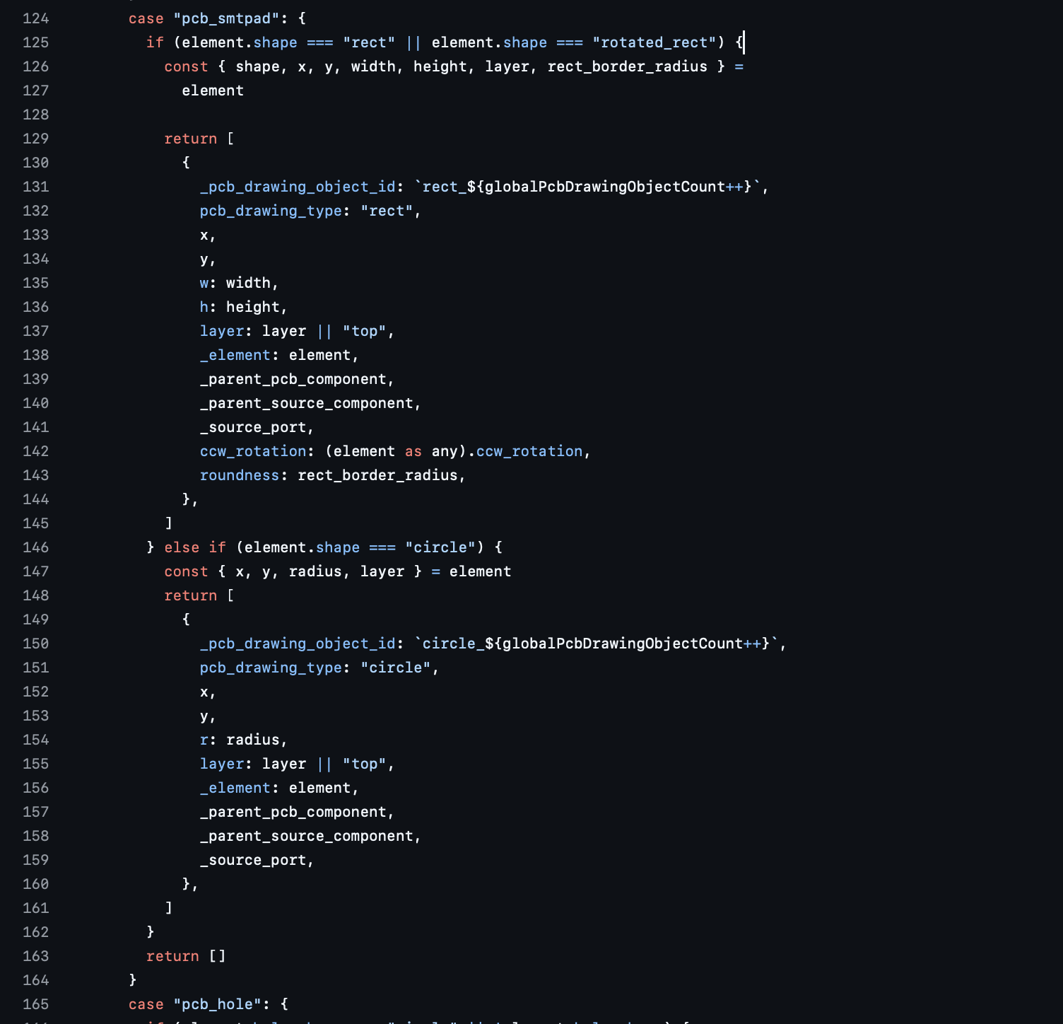
circuit-to-svg/lib/pcb/svg-object-fns/create-svg-objects-from-smt-p...
Convert Circuit JSON into an Schematic/PCB/Assembly SVGs - tscircuit/circuit-to-svg
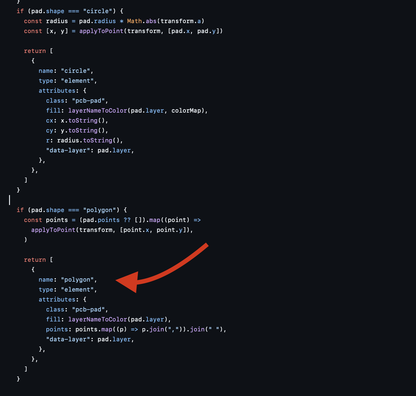
I think we already supported
i mean part of the issue is to just get polygon smtpads working, idk what's currently implemented or not, i just want it to work for the user
@Seve
GitHub
Add example usage of polygon <smtpad /> by AnasSarkiz · Pull Reque...
/claim tscircuit/tscircuit#786
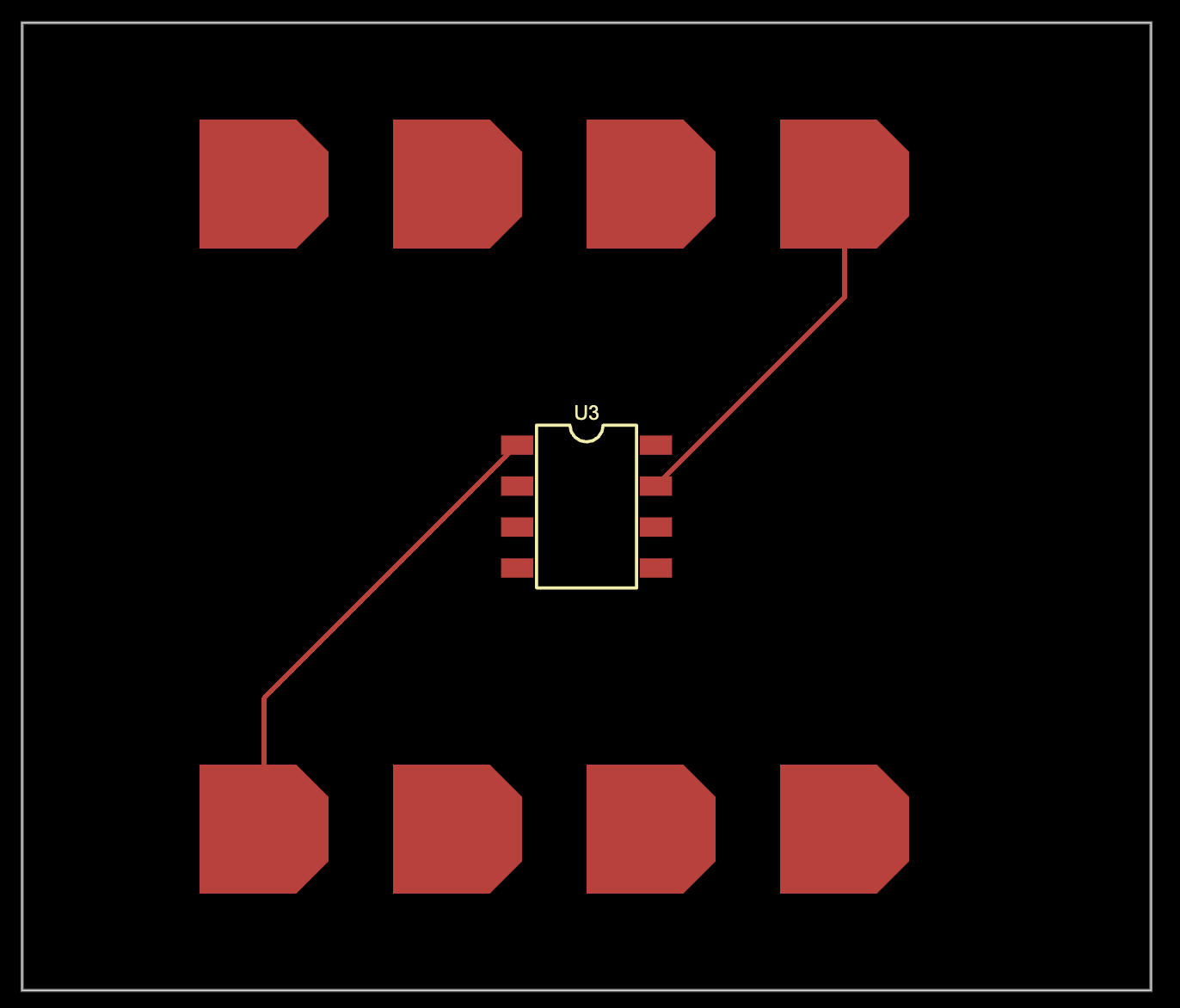
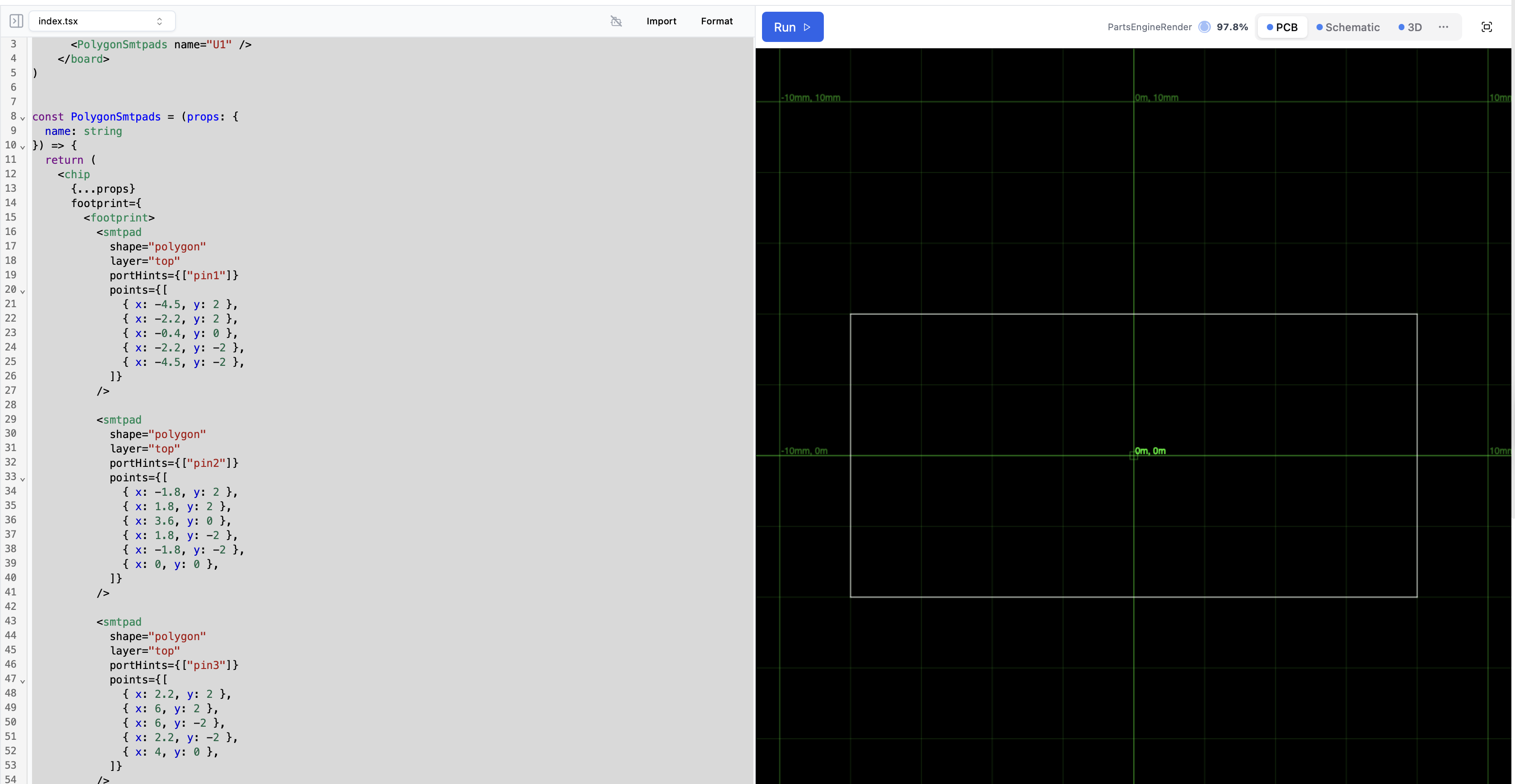
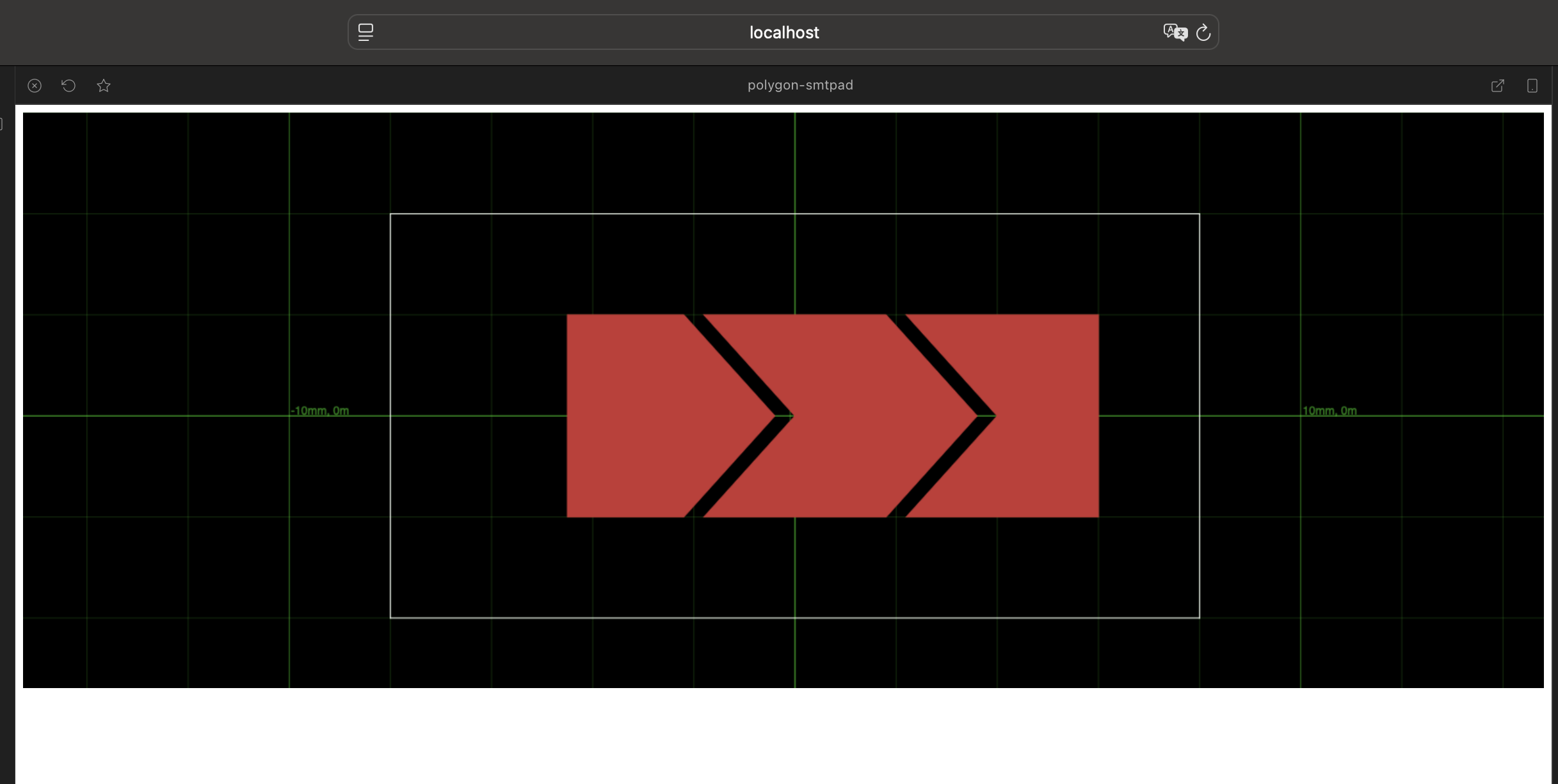
I'm going to be a tiny bit anal and say the shapes are too far off from a capacitive touch string 😁 . The nice thing about this approach is we can see if we get any "bad errors" because they have bounding box overlap
Should I make a full board or just the pads?
Just the pads is find
*fine
@Seve

yep that's correct
looks great
also a great example for the docs
GitHub
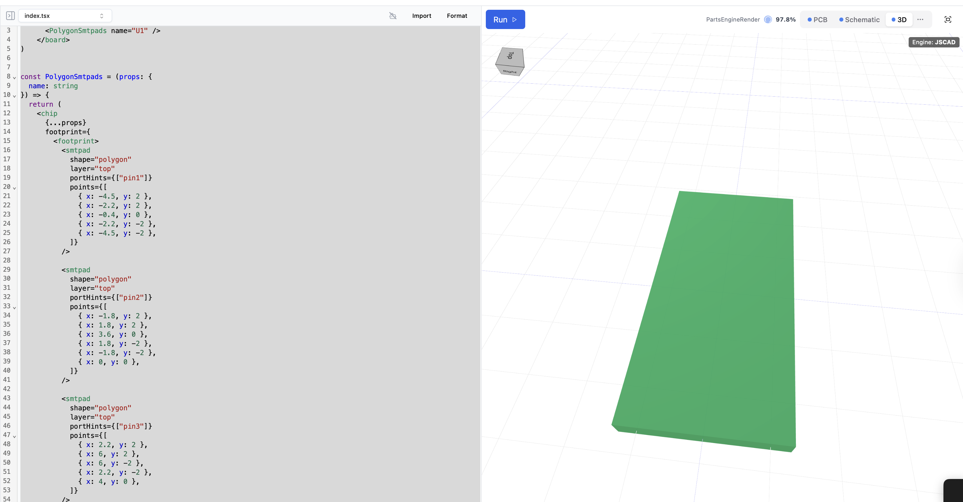
Added test PCB board with a custom polygon-shaped SMT pad by AnasSa...
first step for tscircuit/tscircuit#786
In the docs example, should I make a full example (board with a chip that has three polygon pads)?
@Anas can you clarify, were polygon smtpads working just didn't have a test? did you need to adjust any implementation etc.
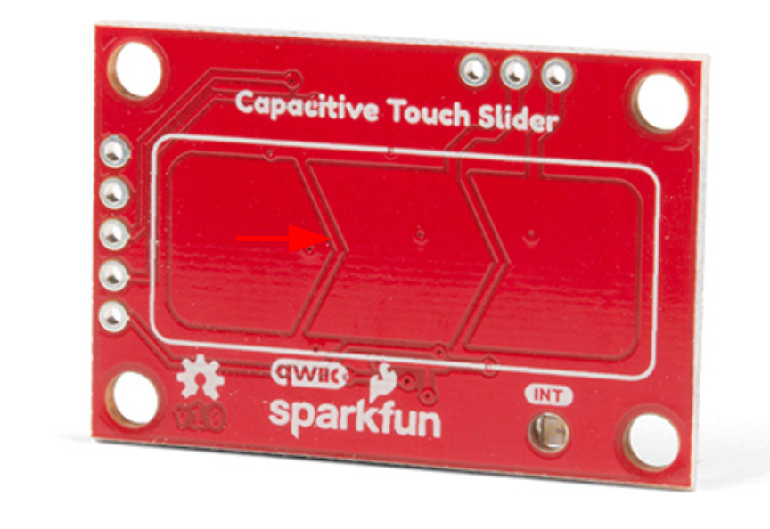
yea i think the three polygon pads is a good example, since people recognize capacitive strips, you could do both, your existing example as the simple example, then add a section with a "Example: Capacitive Touch Strip"
it seems like the polygon smtpads were working so this PR was mostly adding a test and doc? Is that right?
Yes, I think that, I've modified the docs smtpad page, added a polygon with an example in this pr
https://github.com/tscircuit/docs/pull/148
GitHub
Add example usage of polygon <smtpad /> by AnasSarkiz · Pull Reque...
/claim tscircuit/tscircuit#786
its a simple example
<smtpad /> | tscircuit docs
The
<smtpad /> element is used to represent a surface mount pad.hehe ok i thought there would be some fixes associated with this, so this is a pretty high bounty for a doc page
can you add the "Capacitive Strip Tutorial" that has the 3 pads inside a
<chip />, i think that'll be fair to claim the bounty
you don't need to write anything, maybe 1-2 sentences, then show the code example and you're good to go
code style adjustments,
<CapacitiveTouchStrip name="U1" />
make sure to include schPinArrangementDo we need to add the other board components? like holes
nope
you do need soldermask though
the soldermask might actually be a problem 🤔
for a capacitive touch strip to work, the copper has to be covered with soldermask, same as traces
we might want to introduce an
<smtpad /> prop like coverWithSolderMask
lmk if this makes sense, the tricky thing about soldermask is i don't think it shows up in circuit-to-svg currentlySo this will be a new issue, I think
i can either cut the bounty for that issue $75 since there were no fixes or increase the bounty $100 to cover the soldermask issue, but the point of the issue was that a user needed a capacitive strip, so documenting something the user can't use is unfortunately not useful
lmk what you'd like to do, i don't usually change bounties but in this case there were no fixes AND the user's issue isn't solved
U r right,I think we have to split the bounty
eh
actually i'm thinking about this more
i think we need to be mindful of intent, and you're not meeting the criteria of the issue to recreate the example design
i'm going to tip your doc $50 for the unrelated improvement, but i'm rephrasing the original issue to more accurately describe the intent
the issue is here and the bounty has been increased to $250 https://github.com/tscircuit/tscircuit/issues/786
GitHub
Support Capacitive Touch Slider element, add solvermask support to ...
circuit-json supports polygon pcb smtpads, but there isn't an example in the docs https://github.com/tscircuit/circuit-json/blob/main/src/pcb/pcb_smtpad.ts Create a tscircuit/core pcb snapshot ...
tip not working

?
Idk, but I'm not receiving the tip, also the algora comment looks strange
i paid via that stripe link so you should get it
oh we exceeded our algora budget
you should get it now
thnx
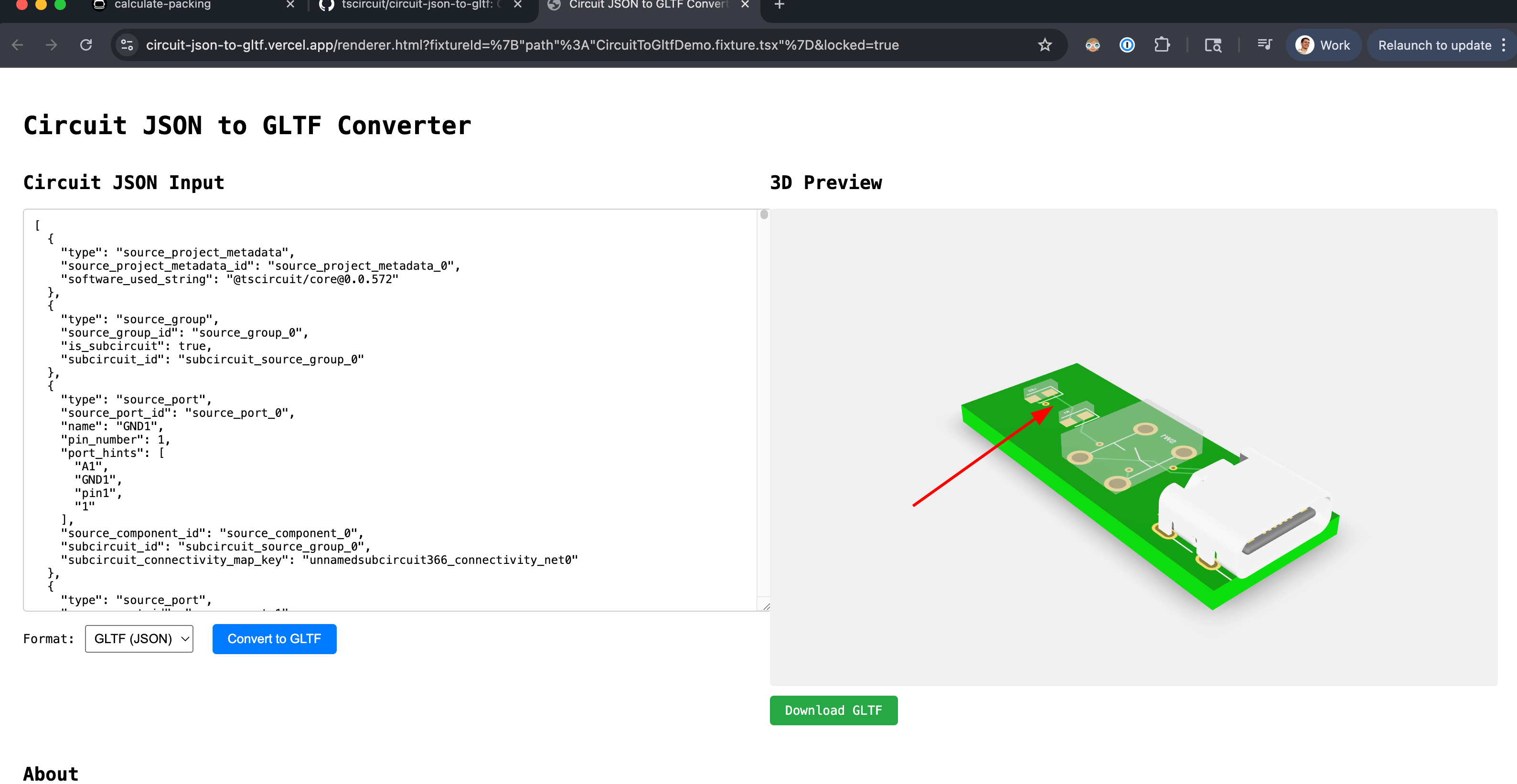
Seve, I'm trying to run my code on tscircuit.com.
3D and PCB viewer do not support polygon SMT pads, or maybe we need to update the dep
ah so the original issue was valid
if you create issues on those repos i'll bounty them
ok, let me check first if the 3D-viewer and PCB-viewer repo support the polygon pads or not
if not Iwill make issue
I found this in 3D-viewr
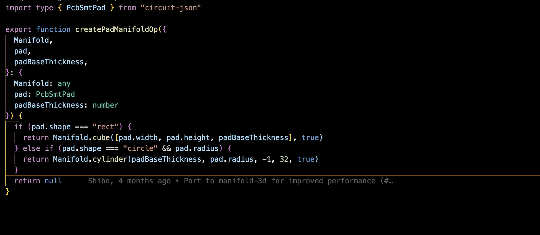
nice yea looks very incomplete
tbh we should be texturing the top of boards rather than performing manifold operations to recreate shapes
so let's create an issue to texture the 3d model rather than continue adding on new manifold shapes
this is an example of a textured 3d model
yeah we need that
also the PCB-viewer not support it
I will create issue
445 commits behind long time 🤕
GitHub
feat: add polygon shape support for pcb_smtpad by AnasSarkiz · Pul...
Implement polygon shape rendering for SMT pads
Add example fixture demonstrating various polygon pad configurations
/fixes #376
/claim #376