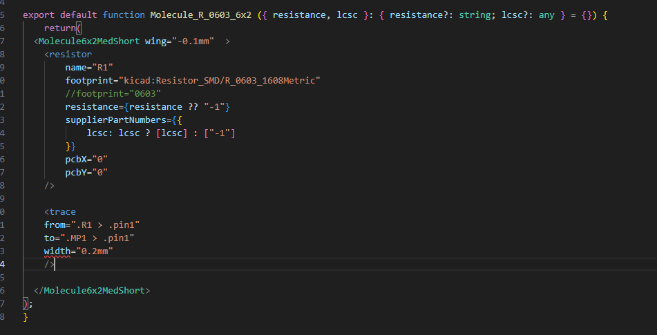
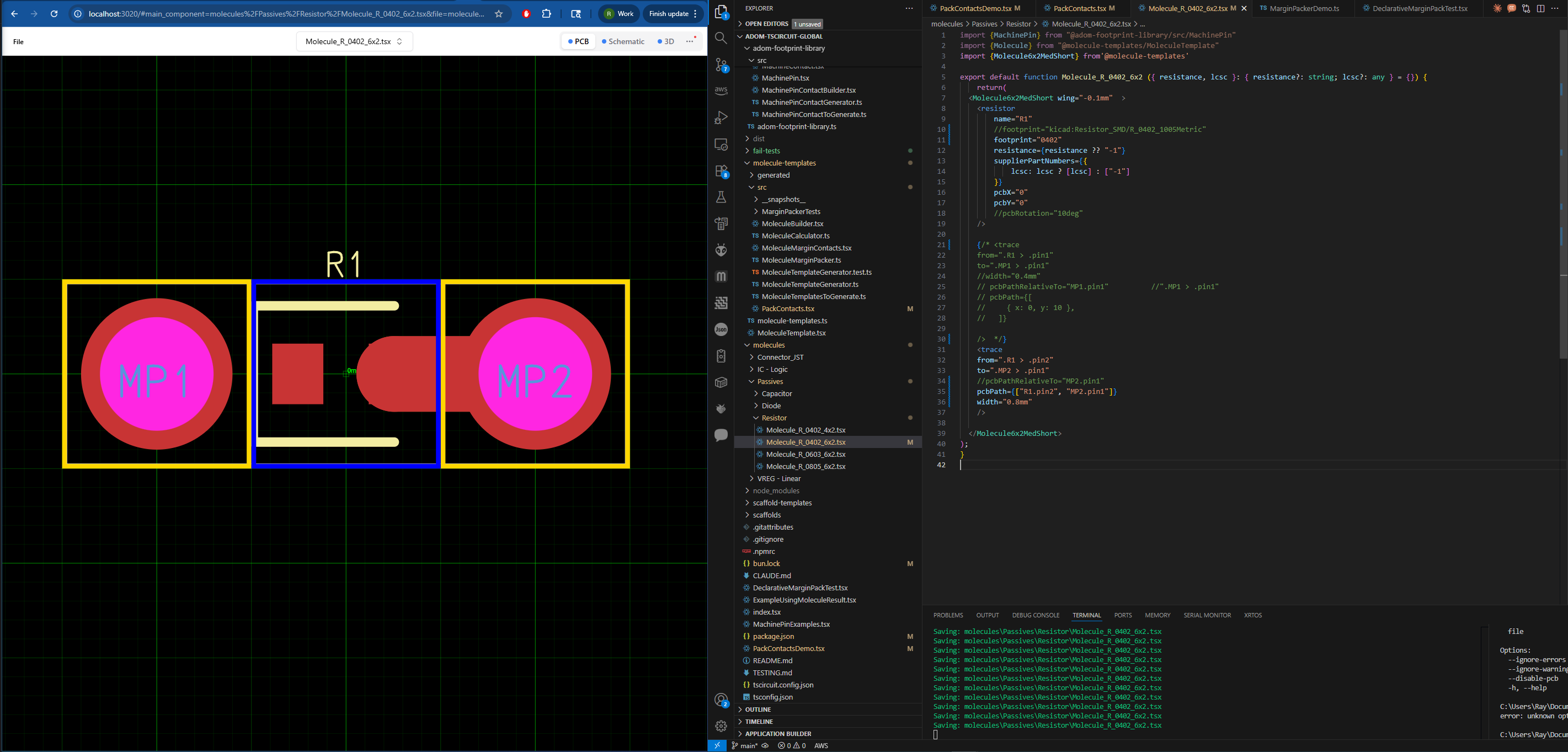
Ray Kholodovsky - <trace from=".R1 > .pin...
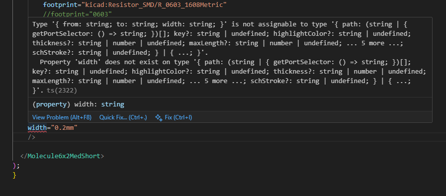
this doesn't appear to be making a trace at all? and width is giving me an error?
trying to follow basic docs here:
https://docs.tscircuit.com/elements/trace#net-vs-direct-connections
<trace /> | tscircuit docs
The
<trace /> element represents an electrical connection between two or more points in your circuit. Traces can connect components, nets, or specific pins on components.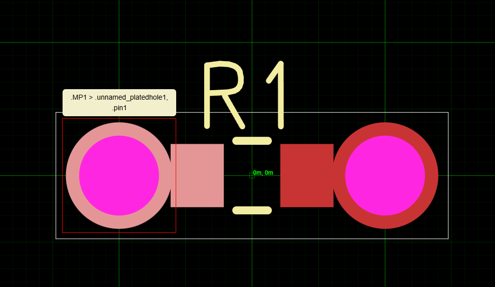
88 Replies
because it's packed so tightly, the autorouter is probably confused (unfortunately)
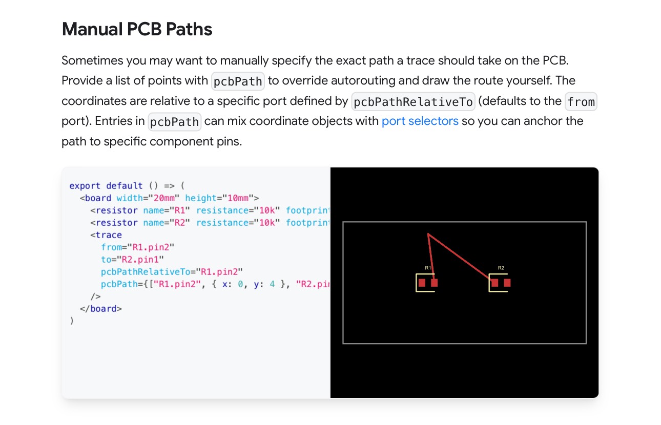
I would specify the trace manually for this particular case https://docs.tscircuit.com/elements/trace#manual-pcb-paths
<trace /> | tscircuit docs
The
<trace /> element represents an electrical connection between two or more points in your circuit. Traces can connect components, nets, or specific pins on components.ok so the trace is rendering after all, and it's just this error with width which does not appear to be respected
width is only respected with the
autorouter="auto-cloud" right now (which uses freerouting). trace width isn't supported yet with the tscircuit autorouter
in general freerouting is a bit more deterministic since it's non-topologicaloh ok.
is there any way I can make things really dumb cuz in this case I literally just need a straight line from A to B with a certain width
yea i would use
pcbPath
you'll just need to specify pcbPath={[{x:0,y:0 }, {x:1,y:0}]}right, and per our earlier convo there's no way that I can query MP1 x and y center positions or more specifically MP1 pin1 center pos to make that easier ?
so because the pcbPath is relative to the pad, I think in this case you would just need to have the
x: traceLength and it should be correct.
there is a feature called route hints that does what you want but yea probably not working with our autorouter
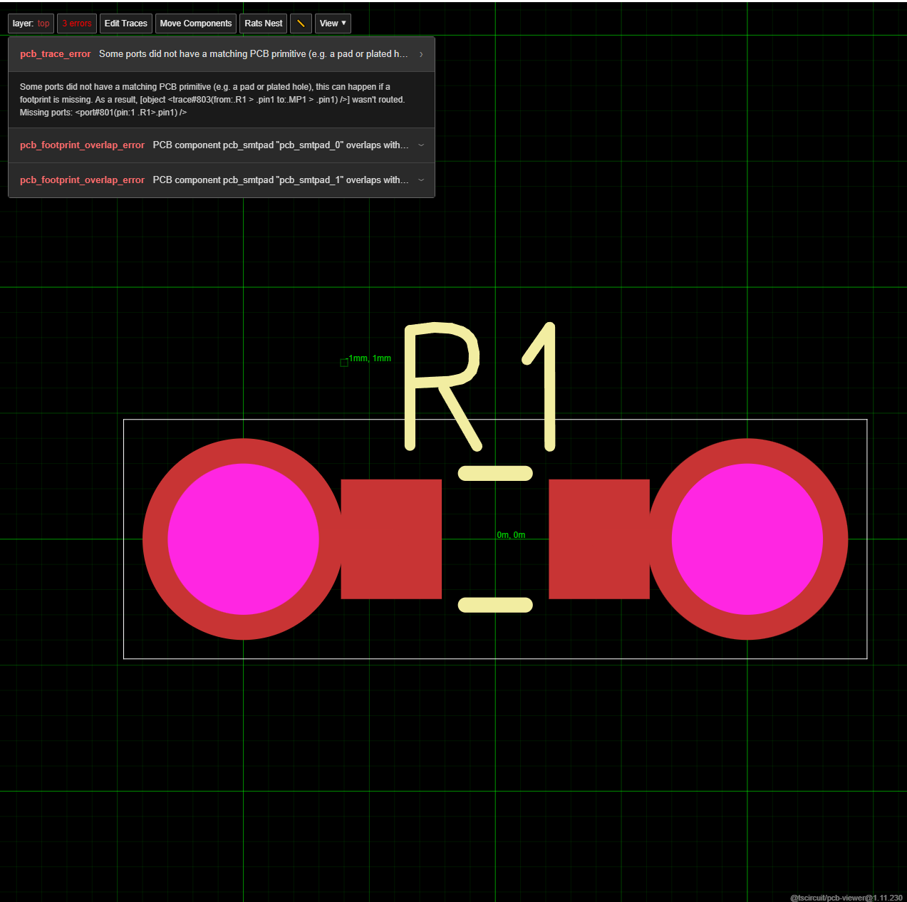
There are basically two issues here, the tscircuit-autorouter doesn't know what to do with overlapping pads and doesn't support trace widthThere are basically two issues here, the tscircuit-autorouter doesn't know what to do with overlapping pads and doesn't support trace widthright, and I actually see those 2 errors for overlap but it's ok for us. It's important to know when to ignore DRC errors 🙂
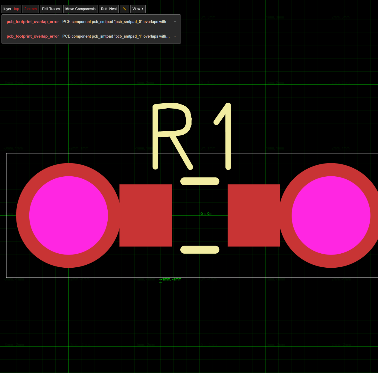
hmm i don't even think it should be throwing those if they are specified as connected 🤔
they aren't specific as connected beyond the <trace I am trying to do.
do I have to do some net thing first?
no doing the trace should be enough
seems like a bug where the connectivity of pads isn't considered for overlap
i mean technically there could be a CAD/Assembly issue but the error should be related to assembly in that case
alright 3 issues
so just trying to draw any trace to see if this pcbPath works and it doesn't like my RelativeTo MP
fixed my syntax mistakes to best of my ability.

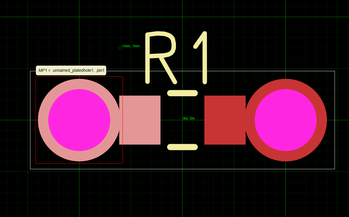
the "port" is the in between guy that my MP is missing?
but I do have a plated hole. so it shouldn't not work
under the hood this is what MP is built as
so there is chip --> footprint -->plated hole
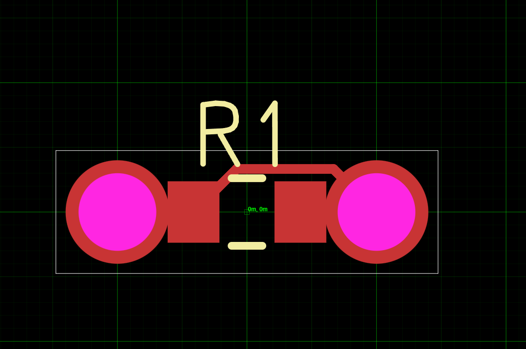
basic traces do appear once I rotated it some.
Not ideal. Are you looking for a particular shape btw, im working on a repro for this in the repo
btw I think even with the overlapping pads traces are still being drawn, they were just impossible to see (without more width) in the original horizontal case.
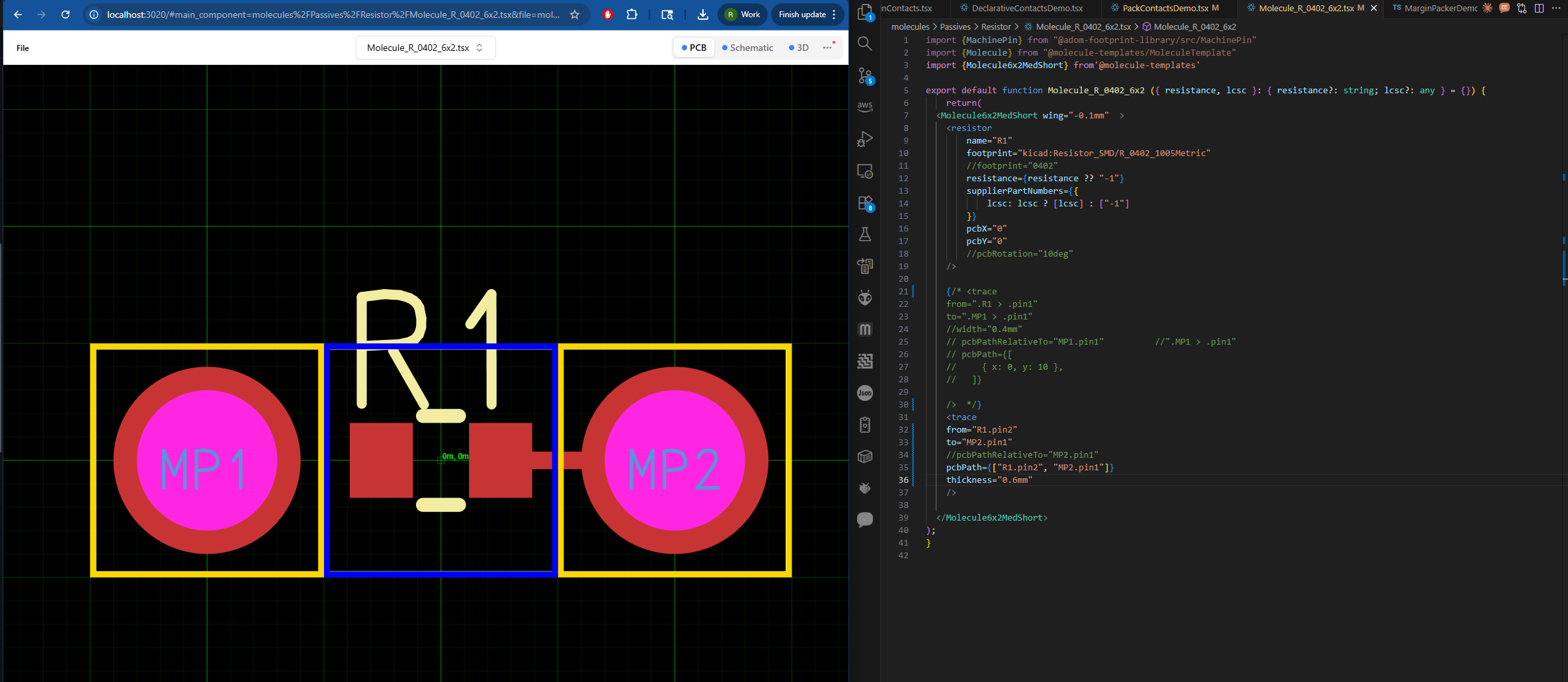
a straight line is all I need here in the original horizontal case
Okay thats better than missing
I think we could potentially support selectors inside pcbPath
That actually seems pretty nice imo
so you would literally say
pcbPath={[{x:0,y:0}, "MP1.pin1"]}inspecting json, I do get traces for each (I think)
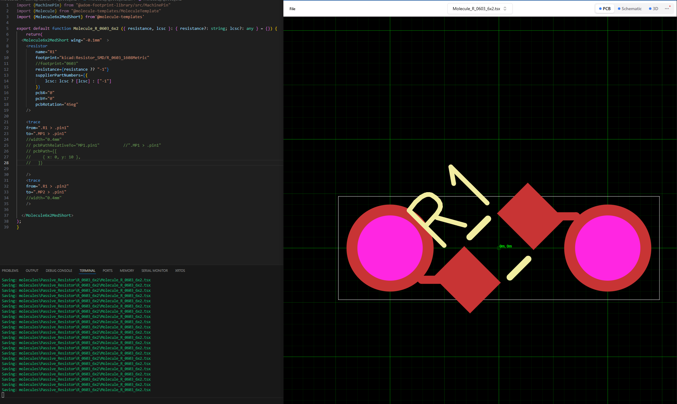
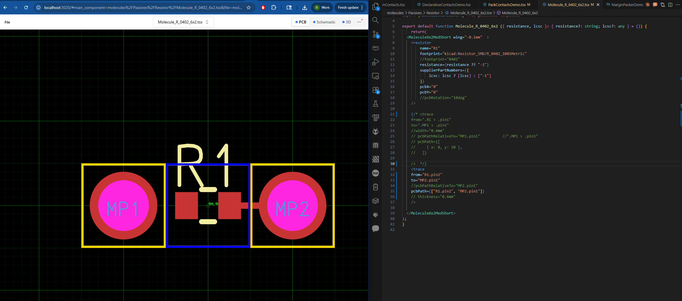
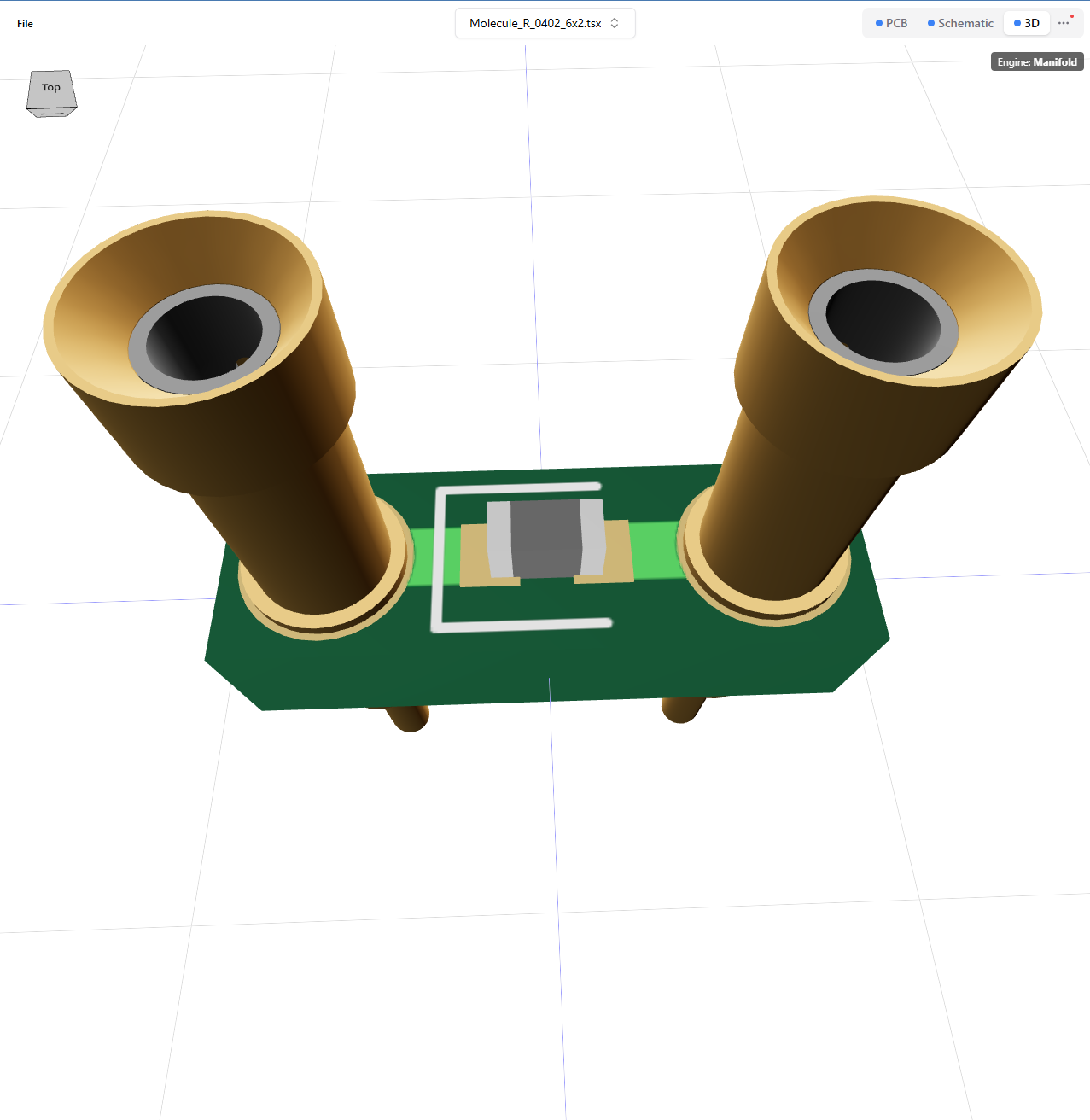
pic1, 10 deg rot
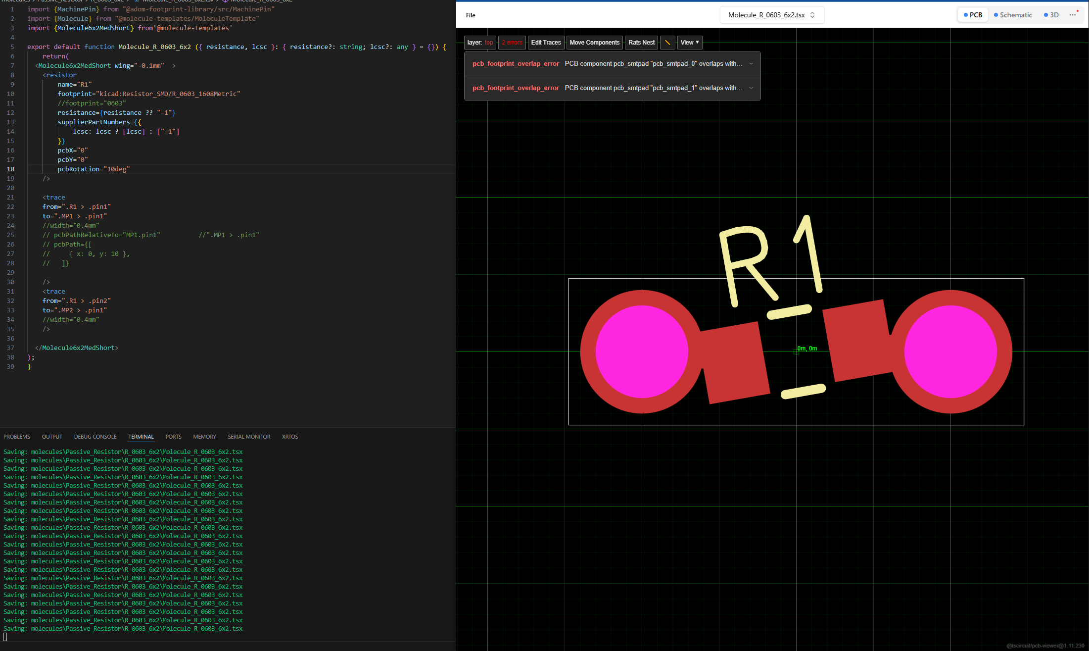
pic2, back to original horizontal no rot
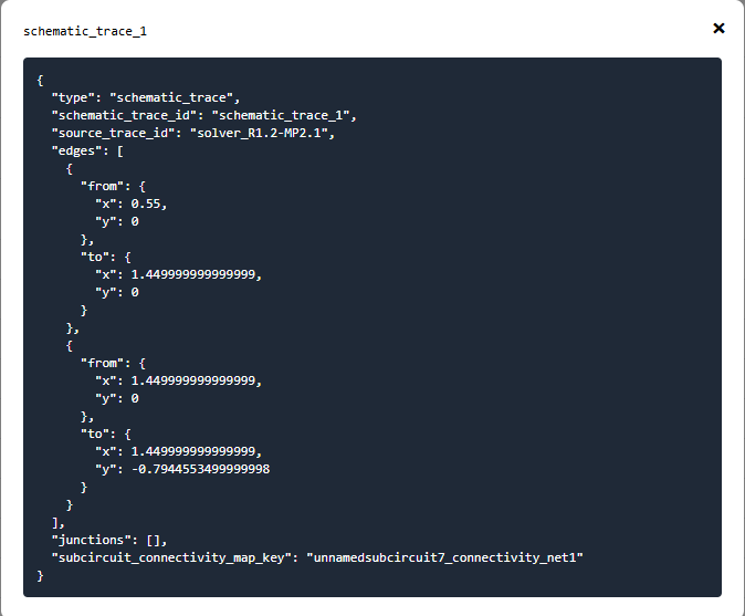
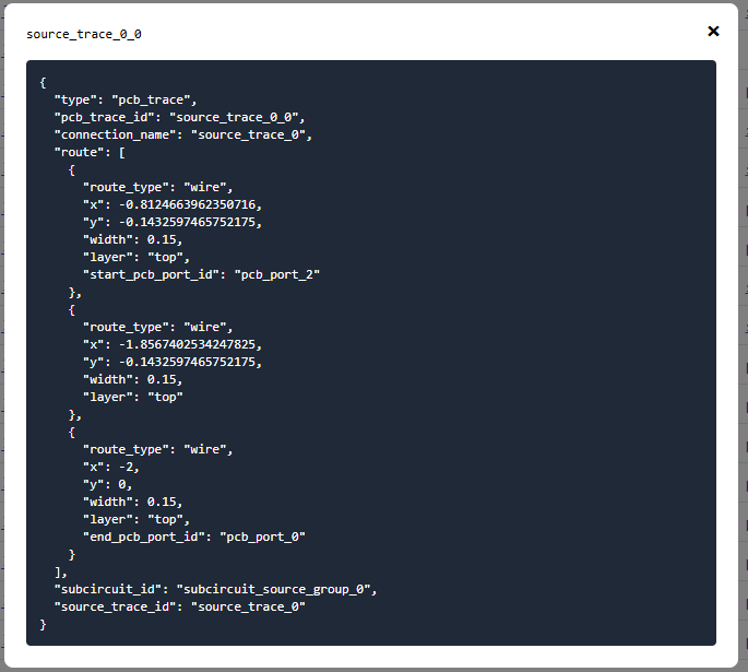
fwiw schematic_trace is different
you need to find the pcb_trace, not source_trace or schematic_trace
it's set up like a SQL database with relational tables, that's why there's different objects for different things
it can be hard to find the appropriate one sometimes
oh. source trace is described as pcb_trace hence my confusion
yea it has references internally
oh right so I just opened the wrong thing for pic 2
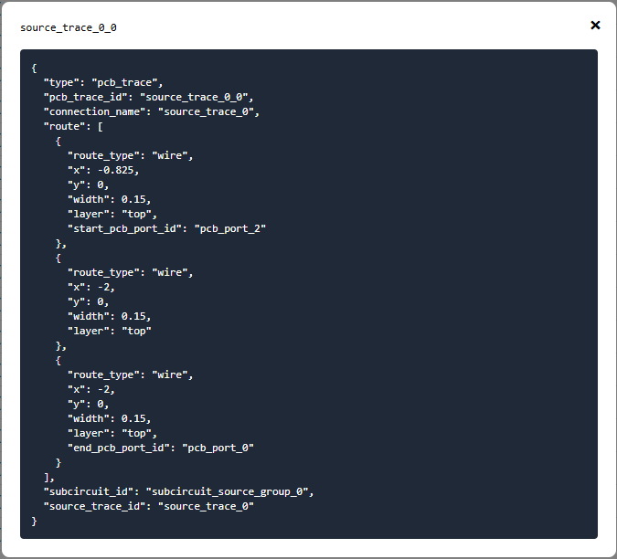
pcb_trace inside source_trace
That title is weird
they appear to be there even in horizontal case. both cases have overlap
Bug in the json viewer…
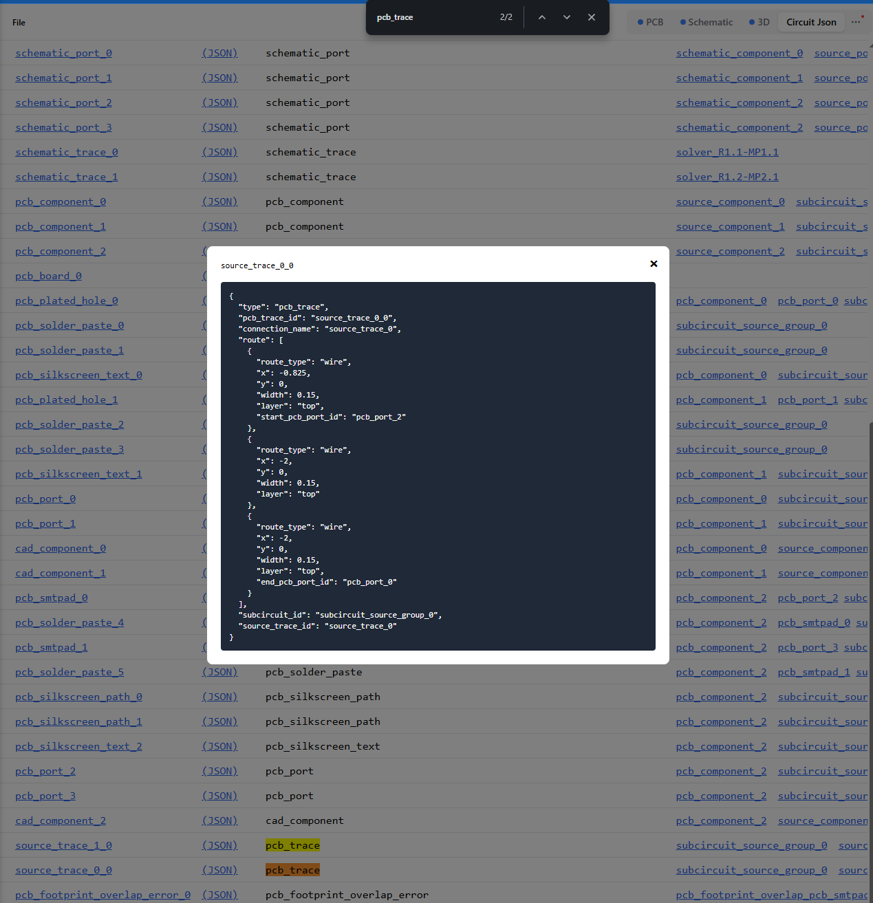
see bottom of white screen:
source_trace_0_0 is indeed what I found / opened
I would ideally want to say
pcbPath={[ {R1.pin1}, "MP1.pin1"] } to indicate a straight line from A to BYea
That seems good
Ok we’ll make it happen, shouldn’t take long
ok so 3 or more issues 🙂
Ill bet @Stéphane Alnet would like this syntax as well
also, it looks like the tscircuit built in router defaults to 0.15mm traces, is there something very "hardcoded built into the logic" like training on that specific size? or could you just pass width down to it somewhat easily?
The hyperparameters for a topological autorouter have to be calibrated for approximate trace widths, we only calibrated for 0.15 atm. We have a couple operations like “trace inflation” that should allow us to have mixed trace widths
understood
I cheated, I used
{x:0,y:0} to get straight paths 😉pcbPath with selectors is now supported !
I’m trying to get a better handle on ports and port selectors so I’m reading this:
https://docs.tscircuit.com/guides/tscircuit-essentials/port-and-net-selectors
I’m confused about whether a component can have a port , like is that the thing that’s in the middle of
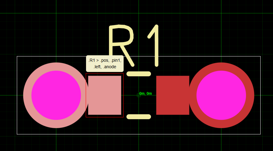
".R1 > .pin1"
that > is allowing you to skip over ?
Port and Net Selectors | tscircuit docs
Selectors are a string used to reference a port, net or any component. They're most
It's CSS selector syntax, I would keep it simple and use the shorthand "R1.pin1" which means "Component name R1 and port name pin1"
it works for any port name e.g.
U1.VCC
> means "direct child of"
the "." means "with a class name of"
our shorthand syntax is not a valid CSS selector, but ai was hallucinating the short form syntax so much we added itright, that is simple and makes the most sense
I was using > because a lot of examples have that, and because in my debugging view the popover shows the in between guy between MP1 and pin1 , for example.
Bu direct child means that > isn't a bridge over the middle guy?
means "direct child of" the "." means "with a class name of"I read the docs 🙂
so the simplest question is do I have to address the
.unnamed_platedhole_1 in between there or can I still say MP1.pin1 ?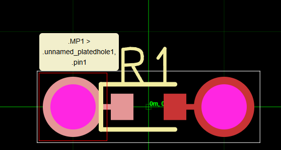
in this case, it's saying that both selectors are valid
but it shouldn't even show the unnamed selector 🤦♂️
Ok so that was the cause of my confusion. I don’t think it was
“Ray needs CSS fundamentals lesson” - although, appreciated, and the docs you quoted are super helpful and relevant
I was trying to understand what a port means in the context of a component in your world.
Cuz in kicad equivalent, my screenshot above would be interpreted as:
“MP1 is a footprint”
The footprint contains a “pad” which in this case is a plated hole.
The plated hole has a pin, 1 pin, named “pin1” or whatever
(I’m going off memory and will double check this at computer shortly)
yea this is changing soon
currently going upstream
it's not going to show unnamed etc.
Ok cool beans then the pedantia doesn’t matter 🙂
ok revisiting this to see if any progress and
these both give me the same result,
and
width="0.4mm" still appears to be an unsupported property. Is there a way I can set a width for a manually defined trace now?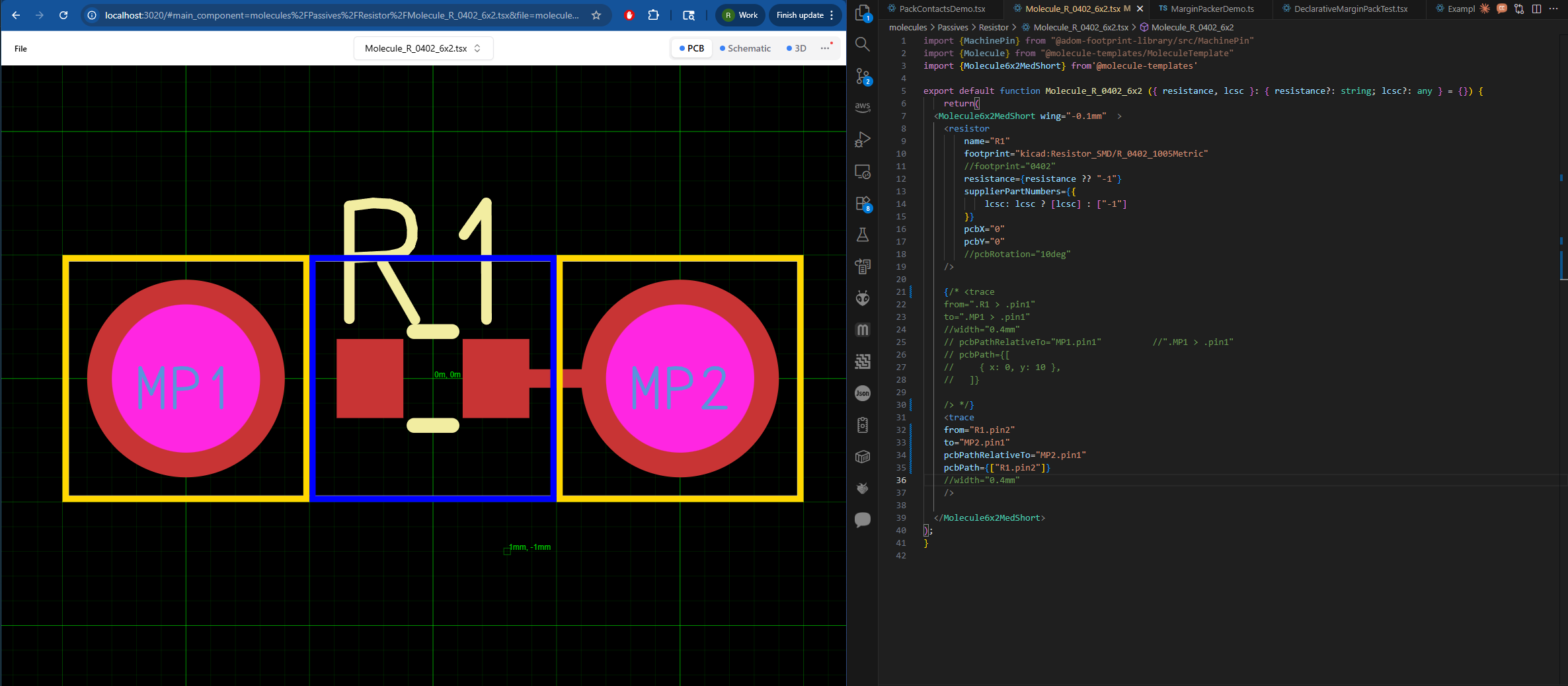
!trace width is supposed to be supported!
taking a look
can you try
thicknessno error but I don't see any change
ok i'm on it
ASAP
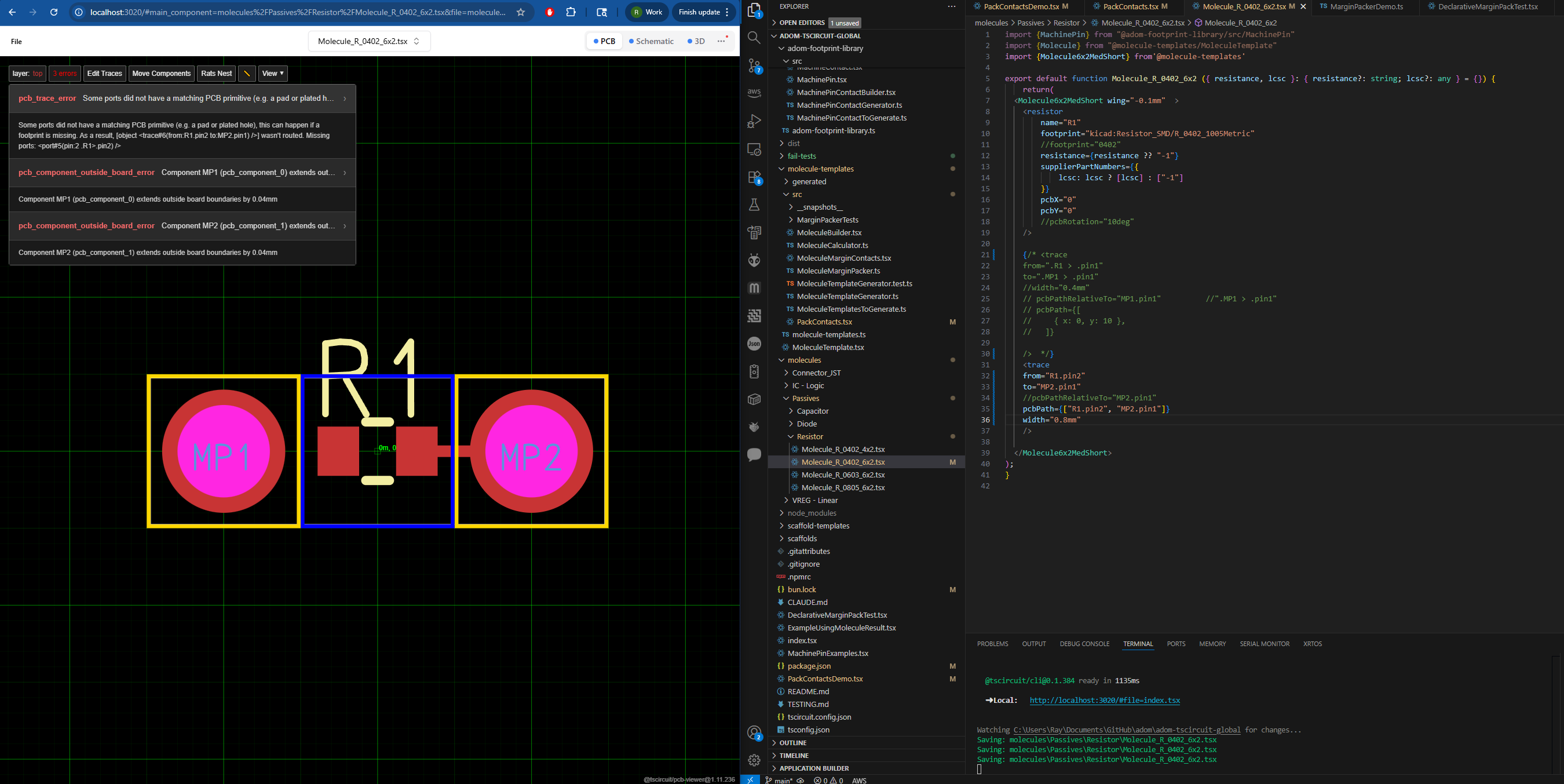
ok so this is dumb but if you add the start and end to your pcbPath (e.g.
pcbPath={["R1.pin2", "MP2.pin1"]}) it will work
i'm patching this but 🤷 that's why it is working in our tests, apparently if a pcbPath doesn't contain 2+ we don't use it(?)I don't see a difference
tried with and without pcbPathRelativeTo
is the pcb viewer possibly stale
fixing all of these issues....
I had already refreshed the window and just did again and commented out the other trace and see that change, to be sure of all
fml
ok sorry about that, lots of fixes coming
although it looks like you have thickness commented out in your screenshot fwiw
yeah was trying a lot of options, screenshot got the tail end of them. (it wasn't working when thickness was in)
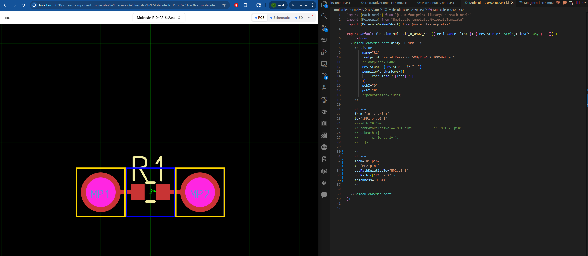
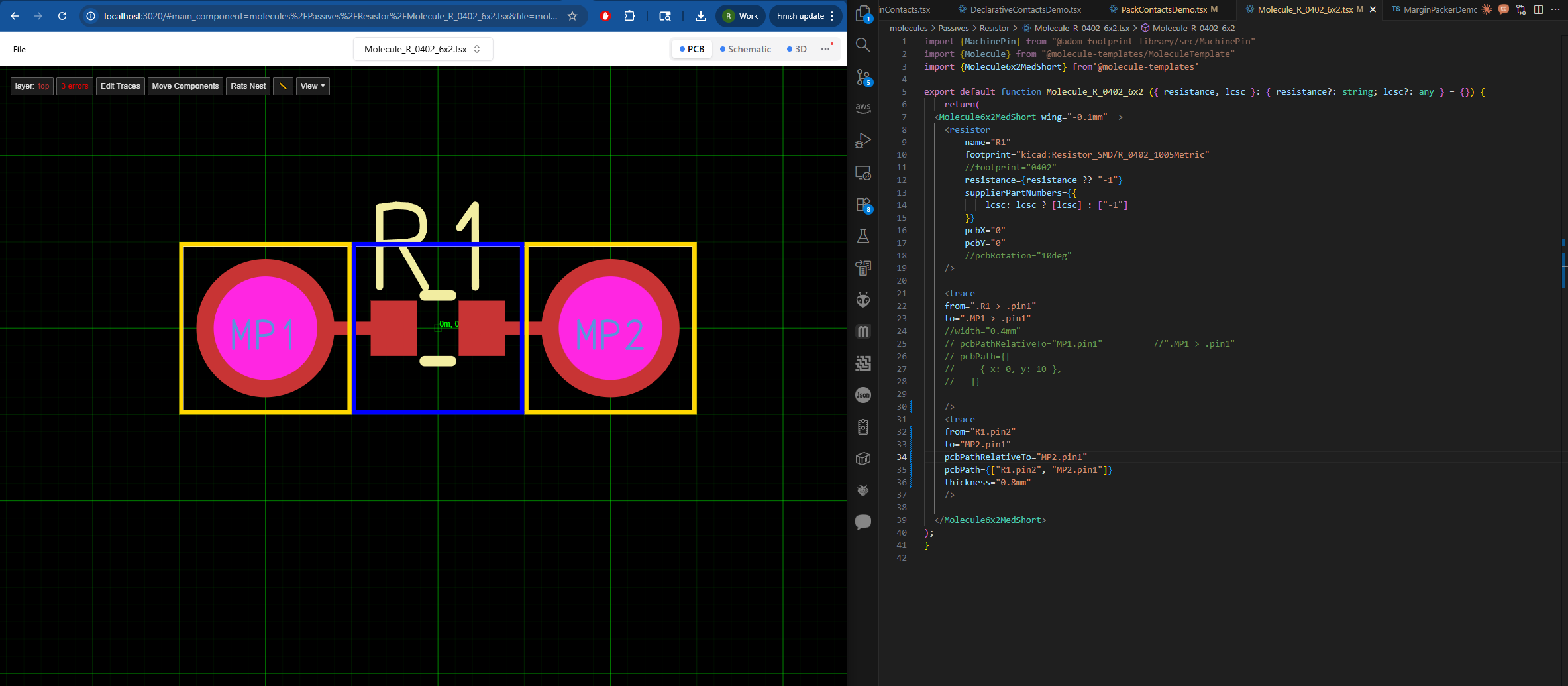
seve I just updated to tscircuit@0.0.809
please be aware of these errors which might be additional clues as to why it's still not working for me. I just submitted a bug report if that helps you.
Thanks yes that is very helpful!!!!
if I go back to the "older" syntax
from=".R1 > .pin2"
to=".MP2 > .pin1"
then I can make the 3rd error go away, I am down to 2 errors, and no change in behaviour.
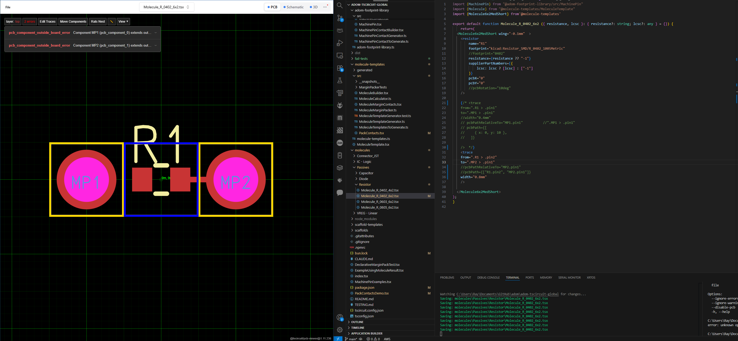
I think that 3rd error, the pcb_trace_error, is kind of outdated/ not actually true in my situation?
like I'm getting the same trace with the same behaviour regardless of which syntax I use,
.R1 > .pin2
or
R1.pin2I wonder if its related to the kicad footprint
boom!
footprint="0402"
AND
pcbPath={["R1.pin2", "MP2.pin1"]}
and width changes
😕 ok so seems like a selector resolution problem with kicad footprints

temporarily happy for now 🙂
Will get that sorted asap, easily defined issue!!!!
woohoo!
@Linear make an issue
I have no idea if that works
making the robots do our bidding, I see
One more try
Could not find the provided team. Be sure to select one from the suggested options.
I'll write your issue by hand, which repo?
You can create any issue against the tscircuit/tscircuit repo
We’ll transfer as needed
ok not synced to github tho 🤔
GitHub
selector resolution problem with kicad footprints · Issue #1149 ·...
related to manual trace width working, discord here: https://discord.com/channels/1233487248129921135/1428459318520447016/1431093507535405067 width change successful with footprint="0402"...
@Seve is there any issue isn't solved (I'm looking for issues)
@Abse yea there's tons of issues, will get you a good one in a sec. But also consider doing some reviews which also gets you contribution points!!
ok
In general I could use a hand verifying the GLB and STEP export is working end to end
https://github.com/tscircuit/tscircuit/issues/1075
Also I think we've introduced a LOT of new circuit-json features that don't have Gerber export and would love it if someone could test that before it becomes a user reported issue
e.g. I'm not sure if properties like
is_cover_with_solder_mask work or if hole_offset_x works etc.GitHub
circuit-json-to-gltf models aren't rotated properly when importing ...
(To replicate, export a GLB from RunFrame)
GitHub
GitHub - tscircuit/circuit-json-to-gerber: Convert Circuit JSON to ...
Convert Circuit JSON to Gerber. Contribute to tscircuit/circuit-json-to-gerber development by creating an account on GitHub.
before it becomes a user reported issuethe user in this example likely being me 😁
I will check it end to end + that will make sure it's ready to order the RP2040 boards when ready
tyty