Commandar Rick - Added test to demonstrate copp...
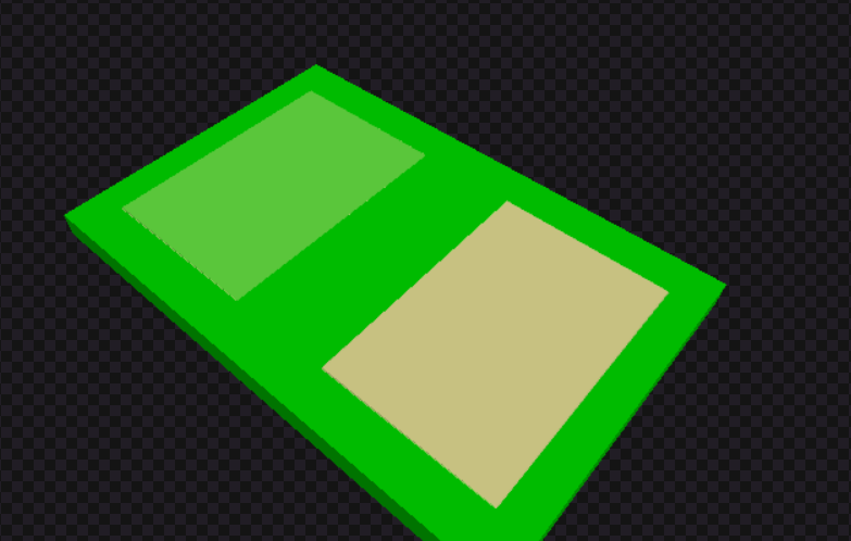
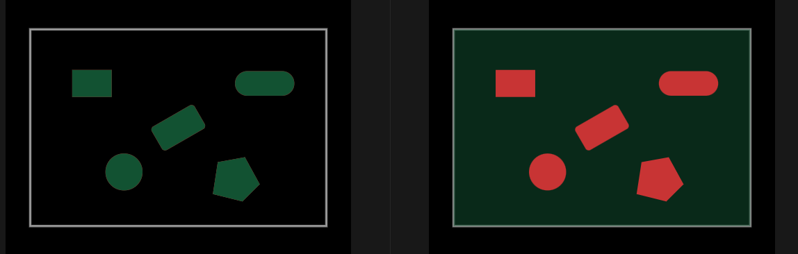
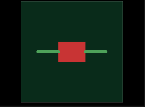
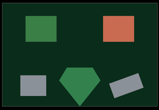
Added test to demonstrate copper pour soldermask differentiation. The rendering already works correctly:
Left: covered_with_solder_mask: true renders as green (soldermask color)
Right: covered_with_solder_mask: false renders as tan/copper (exposed copper)
is this correct?
@shibo
94 Replies
cool, let's make a PR
okay on it
hey so, i think i made a mistake here, once the changes removing the 3d copper pour rendering were removed i kinda forgot to update so the earlier snapshot is using 3d geometry which is wrong, Now that 3D copper pour rendering was removed, the texture rendering (which comes from circuit-to-svg) is not differentiating between copper pours with and without soldermask. Both are rendering the same.
The fix needs to be in the circuit-to-svg library - it needs to check the covered_with_solder_mask property and render accordingly. But we can't fix that here without making it 3d geomentry since it's an external library.
should i try and change the rendering in circuit-to-svg first then update here?
@shibo
i am trying to add minimal 3d geometry to try and fix this here only
https://github.com/tscircuit/circuit-json-to-gltf/pull/89/files
see this
this seems to be an issue tho lemme look into it

i think we might have to fix this in circuit to svg directly as adding 3d geometry rendering to differentiate between copper pours with and without soldermask is causing this rendering issue.
lemme look into it
what does 3d geometry have to do with it? Didn't we already remove the copper pour 3d geometry?
yes we did, but it was the 3d-geometry that was differentiating between copper pours with and without soldermask. since we moved to a textures only approach using circuit-to-svg, the fix needs to be in the circuit-to-svg library - it needs to check the covered_with_solder_mask property and render accordingly.
i dont think so it currently does
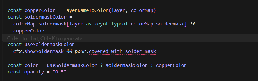
I've adjusted the code to set the opacity of copper pours to 0.2 if covered by solder mask and 0.5 if not.

this should fix the issue
@shibo
@Seve how do we represent soldermask in the pcb-viewer?
It should be shown if the user toggles on “Show Solder Mask”
Do not change the opacity of copper pours in relation to solder mask
@Commandar Rick see how kicad does it
so what i did is set it to 0.5 if show solder masks is on, (which is what it was before) and set to 0.2 if its off thats the only logic i added
okay lemme see
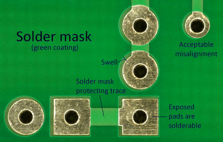
@Commandar Rick looks like we represent soldermask using a green color
check circuit-to-svg examples
so sm like this
this checks the show solder mask property and sets the colour automatically without changing the opacity
@shibo i can put a pr for this heres the logic
also this fix is in circuit-to-svg
hmm, I believe it was already implemented but only showed up when using a specific flag
I'm debating whether we should show soldermask always in the gltf
I discussed this a bit w/ @Rishabh , but solder mask shouldn't show without the flag, and currently circuit-to-svg is not drawing solder mask over the board which is a bug
In the GLTF, solder mask should always show, but it looks weird because of the bug i'm mentioning above
nobody is working on the bug afaik, but Rishabh also understands the issue fwiw
@Commandar Rick do some comprehensive testing in circuit-to-svg using the
showsoldermask flag to make sure it works correctly, then we'll enable the flag in circuit-to-gltfokay on it
I've confirmed the bug Seve mentioned. The solder mask was not being drawn over the main PCB board itself; it only appeared on copper pours. This made the feature look broken when the showSolderMask flag was enabled.
I've fixed this by updating the board rendering logic in circuit-to-svg. The renderer now draws a filled solder mask layer over the entire board when the showSolderMask flag is used.
With the showSolderMask flag enabled, the solder mask (the green area) now correctly covers the entire surface of the board. Is this the correct behaviour?
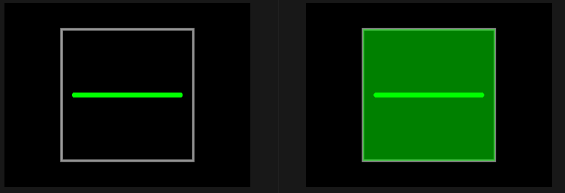
before and after
It’s not correct because youre drawing the solder mask twice
You may need to use flatten-js/core for this im not sure
is this better? @shibo
idk myself
you still want soldermask on top of the pads
but for that we will have to draw them twice which seve said is an issue
or maybe i miss understood
Dont make solder mask transparent
Solder mask with pads underneath is a different color
Boolean geometry fixes this 100x better
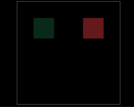
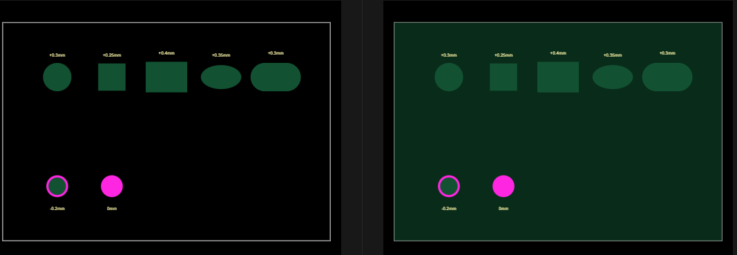
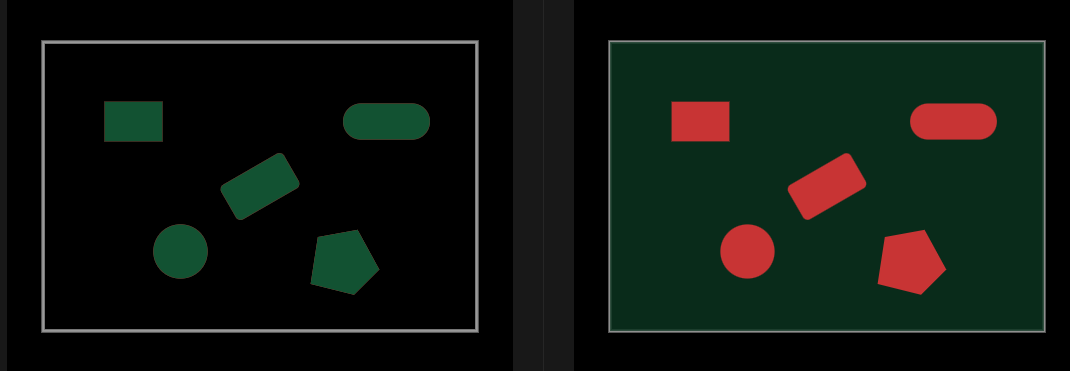
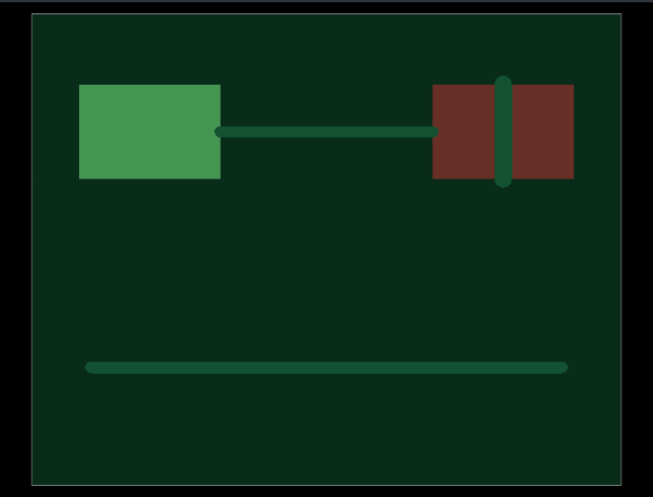
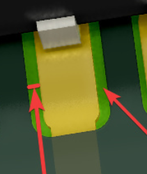
something like this, when copper is covered with soldermask there is a distinct color
yes in shibo's pic there, you can see three colors:
- copper pad (silver)
- Light green (solder mask with copper)
- Darker green (solder mask w/o copper)
opacity is very unlikely to achieve the desired results with coloring
in this test add some pads that aren't covered with soldermask, regular soldermask will be dark green, soldermask on pads will be light green, and none covered pads will keep their color
@shibo i do feel like we should have something like
circuit-json-to-geometry that simplifies the process of converting circuit json into geometries for operations like this
that logic would be reusable as wellokay cool understood thanks for this, i think this will be really helpful
but that's for the future
you can use flatten.js to subtract pad shapes from the soldermask
flattenjs has Polygon.svg() which should make geometry testing very easy- this could also be useful for lightburn and GLTF cutouts etc. as we add new stuff light slot paths
https://github.com/tscircuit/circuit-json-to-geometry
I don't think it's necessarily super important right now but I think this module could output various polygon shapes, e.g.
convertPlatedHoleToPolygonGitHub
GitHub - tscircuit/circuit-json-to-geometry
Contribute to tscircuit/circuit-json-to-geometry development by creating an account on GitHub.
is this in the right direction?
some ther test cases with updated snapshots
@shibo
this will also need to implemented for smtpads too right? they seem to broke because of this
this is after the fix extending the logic to smtpads too
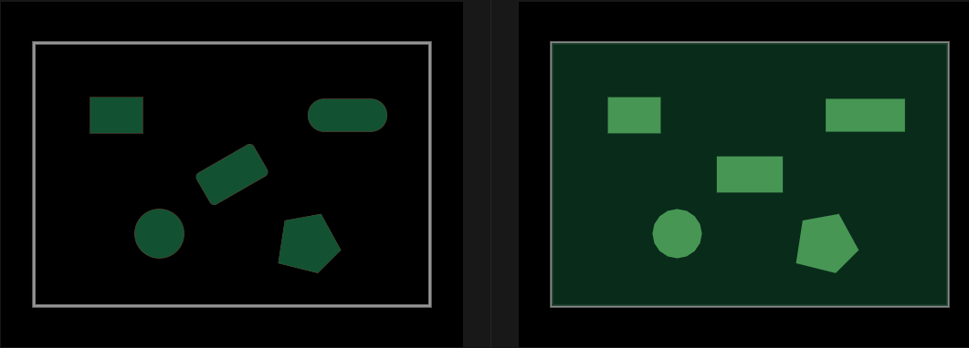
wait i dont think mine is correct, or is mine in the right direction, im a lil lost
@Seve
That is better
should the contrast be more(the board should be darker or the copper pour covered with solder be more brighter?)
It looks about right
Make sure traces work
okay will do there seems to be a bug with the snapshot soldermask-margin-smtpad.snap.svg but looking into fixing this
https://github.com/tscircuit/circuit-to-svg/pull/434
prolly will have a lot of errors
but could be a starting point
@Seve
also added tests for traces
traces should be the same color as pads
both are just copper
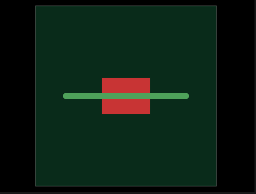
also, there shouldn't be a trace crossing the pad in your test
CC @Rishabh just did some work here, i don't think it's completed but he should be tagged sometimes i think
@Commandar Rick i'm pretty confused looking at your screenshot. Traces have copper underneath them, so they're the same color as pads covered with soldermask.
copperWithSoldermask applies for pads and traces
If a trace is over a pad, then the soldermask for the trace isn't applied so that the pad is completely copper
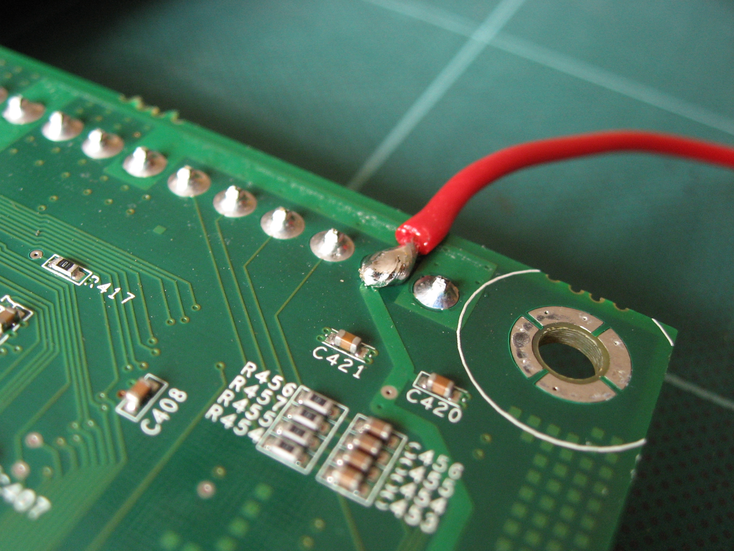
hey just to clarify the trace over the pad should not have solder mask, the trace just over the copper pad should also be exposed right?
fixed this issue
before and after
The trace part which is crossing the pad should not have solermask as Seve said
okay cool so like this ?
Can you try to make it so that it doesn't go into the pad
lemme try
but this is the correct direction right?
Y
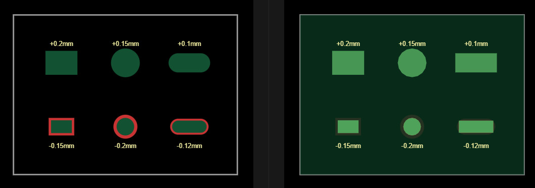
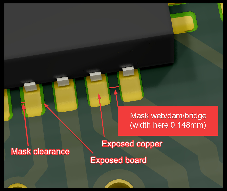
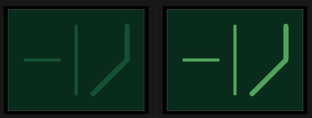
Next step is to have the mask clearance shown in this image
Basically a buffer zone around the pad
yeah but i feel might need to make a seperate pr for that, imo that might be better
To accomodate manufacturing misallignment
Ok
got it got it so just some area around the exposed pads to have a margin of soldermask? sort of like that
A margin of no soldermask yeah
okay okay got it
okay yeah looked a lil closely got it so this right
Yeah
hey @Rishabh , i was also working on the same issue can you please this once
i think your prs https://github.com/tscircuit/circuit-to-svg/pull/435/ and https://github.com/tscircuit/circuit-to-svg/pull/436/ solved a lot of what my pr was trying to can i help in any way?
You were working on the copper pours right?
yes i was working on this, https://github.com/tscircuit/circuit-json-to-gltf/pull/86 and then i was supposed to work differentiating between copper pours with and without soldermask
but i am a little confused rn because as a part of fix for copper pour i was also trying to fix soldermask but i think your pr did that exactly, can you tell me what exactly i should do next?
if my understanding is correct now that your pr solves the bigger picture with soldermasks in general i should focus on copper pours specifically right?
Yes, you can go ahead and work on the copper pour's
okay will put a fresh pr for that
and should i also try to work on this? or is this fixed?
in your pr
I think so, will check with Seve about that
and also the copper pour fix will also be in circuit-to-svg right?
Yes, I think so. Cause I didn't test that
okay will start work on this
hey @Rishabh @Seve @shibo
is this correct
for coper pours
the fix is a lil hacky but is this what we are trying to achieve?
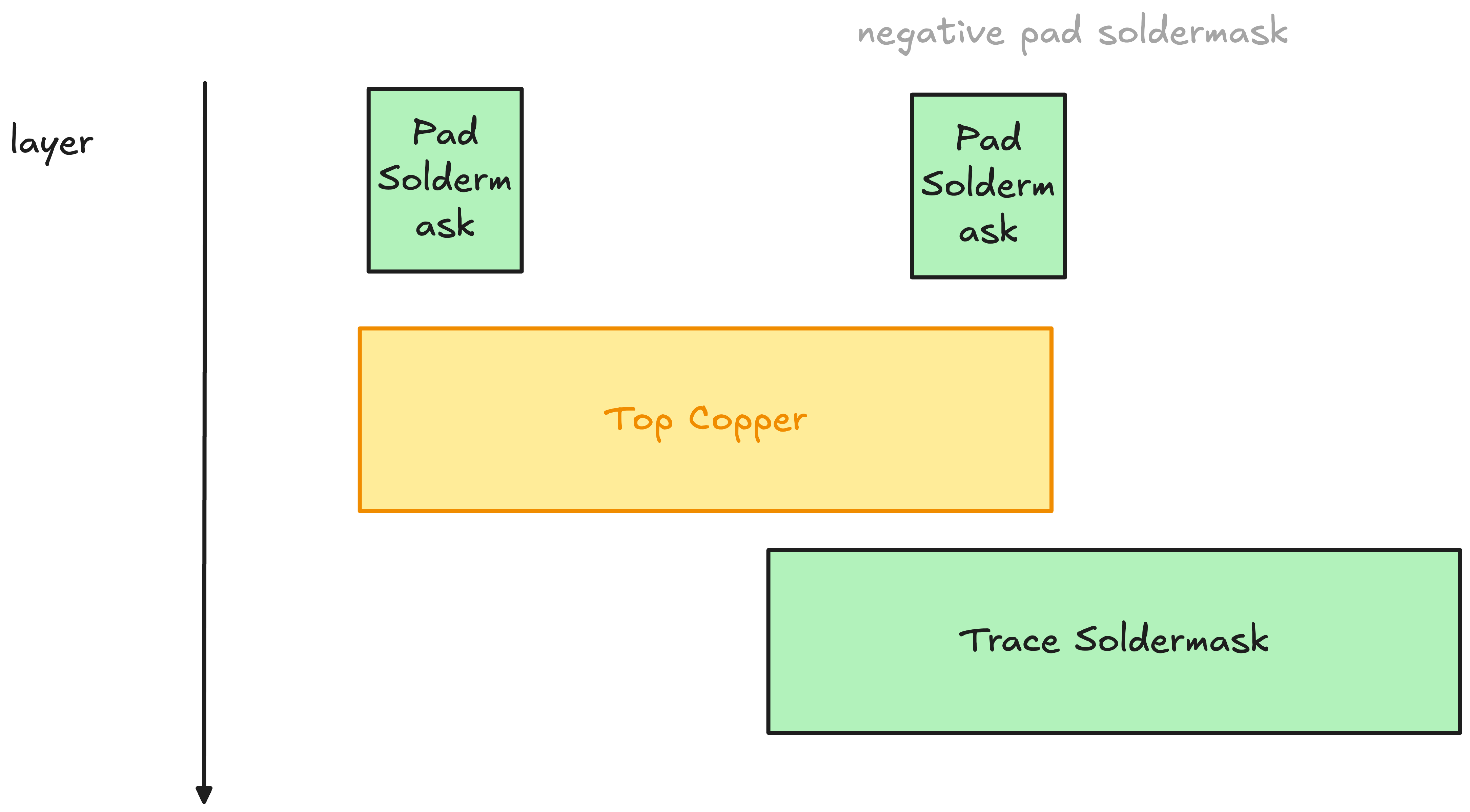
i discussed this this morning w/ Rishabh- we discussed having two layers for solder mask so that it would be easier to get things working without boolean operations
okay will follow this 👍`
is this correct, this uses the two layer approach
what are the gray boxes?
the board material?
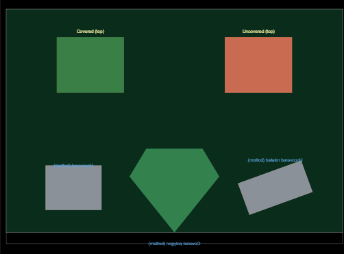
you can add silkscreen text to help the reviewer understand what's going on- that could be very helpful to prevent regressions
above each of the items just say what it is with some small text
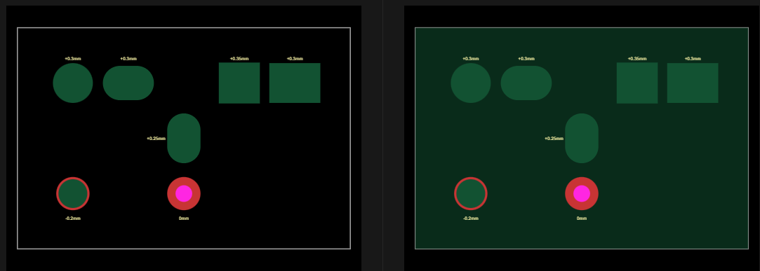
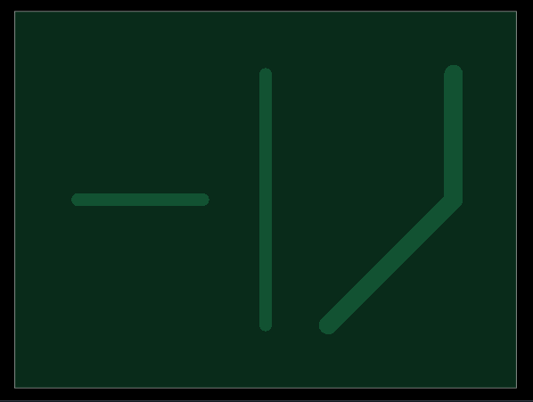
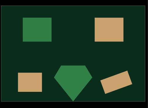
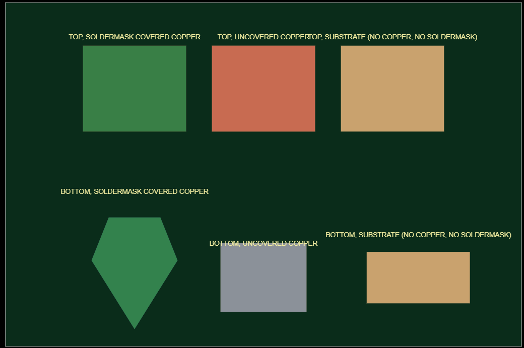
yes the gray boxes are the substrate (board material) showing through pcb_soldermask_opening cutouts where soldermask is removed. Adding silkscreen text labels above each shape in the test:
uh yes that seems good, but i'm confused at your labels, there should be 3 on the top, 3 on the bottom with
- TOP, SOLDERMASK COVERED COPPER
- TOP, UNCOVERED COPPER
- TOP, SUBSTRATE (NO COPPER, NO SOLDERMASK)
is this better?
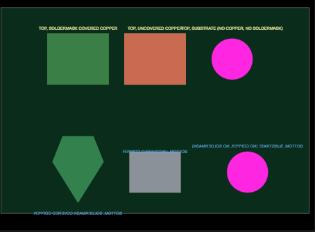
yes, but the bottom is unreadable
why put the silkscreen on the bottom layer?
also why would the substrate show as a drill color? That's definitely wrong
sorry ab that, hows this
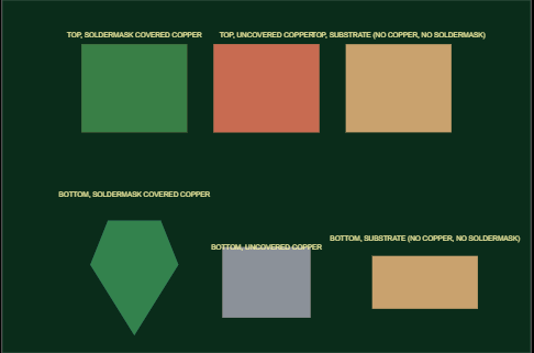
higher res
nice
cool will put a pr for review
https://github.com/tscircuit/circuit-to-svg/pull/438
please check will prolly be full of bugs tho still learning 😭😭
hey @Rishabh can you check this once?
.
updated please see
@Seve i have tried to remove all possible instances of obfuscation i could, hope its better now