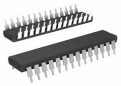
When creating a footprint for a component in my PCB Design, what are some practices I should conside
When creating a footprint for a component in my PCB Design, what are some practices I should consider.
@PCB & Analog
@PCB & Analog


 my name is Manel i have master degree in network engineering and i have some projects in Nextjs firebase tailwind also i recently gratuted from Recoded programme for software development now im working on article about detection of attack in IoT
 @eHamzaDZ Welcome aboard! It's wonderful to see you here. Can you introduce yourself and tell us what you do professionally?